
Page 136 - Complete Wireless Design
P. 136
Amplifier Design
Amplifier Design 135
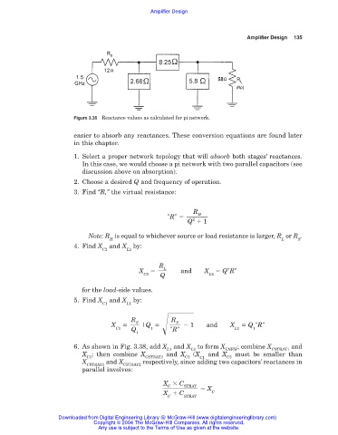
Figure 3.35 Reactance values as calculated for pi network.
easier to absorb any reactances. These conversion equations are found later
in this chapter.
1. Select a proper network topology that will absorb both stages’ reactances.
In this case, we would choose a pi network with two parallel capacitors (see
discussion above on absorption).
2. Choose a desired Q and frequency of operation.
3. Find “R,” the virtual resistance:
R
H
"R"
2
Q 1
Note: R is equal to whichever source or load resistance is larger, R or R .
H L S
4. Find X and X by:
C2 L2
R
L
X and X Q"R"
C2 Q L2
for the load-side values.
5. Find X and X by:
C1 L1
R R
S
S
1
X |Q and X Q "R"
C1 Q 1 "R" L1 1
1
6. As shown in Fig. 3.38, add X and X to form X ; combine X and
L1 L2 LNEW CSTRAY1
X ; then combine X and X (X and X must be smaller than
C1 CSTRAY2 C2 C1 C2
X and X respectively, since adding two capacitors’ reactances in
CSTRAY1 CSTRAY2
parallel involves:
X C
STRAY
C
X
X C C
C STRAY
Downloaded from Digital Engineering Library @ McGraw-Hill (www.digitalengineeringlibrary.com)
Copyright © 2004 The McGraw-Hill Companies. All rights reserved.
Any use is subject to the Terms of Use as given at the website.