Page 140 - Complete Wireless Design
P. 140

Amplifier Design


                                                                               Amplifier Design  139


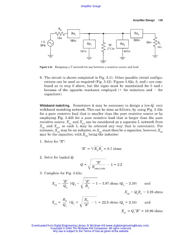
                        Figure 3.40 Designing a T network for use between a resistive source and load.


                        9. The circuit is shown completed in Fig. 3.41. Other possible circuit configu-
                           rations can be used as required (Fig. 3.42). Figure 3.42a, b, and c are com-
                           bined as in step 8 above, but the signs must be maintained for  b and c
                           because of the opposite reactance employed (  for inductors and    for
                           capacitors).


                        Wideband matching. Sometimes it may be necessary to design a low-Q, very
                        wideband matching network. This can be done as follows, by using Fig. 3.43a
                        for a pure resistive load that is smaller than the pure resistive source or by
                        employing Fig. 3.43b for a pure resistive load that is larger than the pure
                        resistive source. X  and X  can be considered as a separate L network from
                                         S1      P1
                        X   and X , so each L may be oriented any way that is convenient. For
                          S2      P2
                        instance, X may be an inductor, so X must then be a capacitor; however, X
                                   S1                      P1                                  S2
                        may be the capacitor, with X  being the inductor:
                                                   P2
                        1. Solve for “R”:
                                                "R"    R R    8.7 ohms
                                                          S  L
                        2. Solve for loaded Q:

                                                         "R"
                                                Q                 1   2.2
                                                       R
                                                        SMALLER
                        3. Complete for Fig. 3.43a:

                                      "R"          "R"

                                                         1   3.97 ohms (Q   2.19)
                                X         |Q     		                                   and
                                 P2   Q      2     R                     2
                                        2           L
                                                                          X    Q R   3.28 ohms
                                                                           S2    2  L
                                      R           R
                                                    S
                                       S

                                                        1   22.9 ohms (Q   2.18)
                               X         |Q      		                                   and
                                 P1   Q     1     "R"                    1
                                       1
                                                                        X     Q "R"   18.96 ohms
                                                                          S1   1
                   Downloaded from Digital Engineering Library @ McGraw-Hill (www.digitalengineeringlibrary.com)
                               Copyright © 2004 The McGraw-Hill Companies. All rights reserved.
                                Any use is subject to the Terms of Use as given at the website.
   135   136   137   138   139   140   141   142   143   144   145