
Page 135 - Complete Wireless Design
P. 135
Amplifier Design
134 Chapter Three
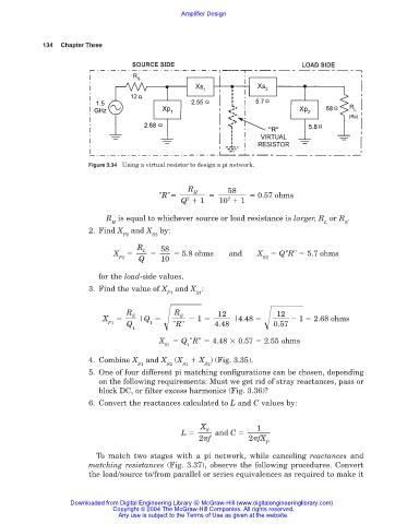
Figure 3.34 Using a virtual resistor to design a pi network.
R 58
H
"R" 0.57 ohms
2
2
Q 1 10 1
R is equal to whichever source or load resistance is larger, R or R .
H L S
2. Find X and X by:
P2 S2
R 58
L
X 5.8 ohms and X Q"R" 5.7 ohms
P2 Q 10 S2
for the load-side values.
3. Find the value of X and X :
P1 S1
R R 12 12
S
S
1
X |Q |4.48
1 2.68 ohms
P1 Q 1 "R" 4.48 0.57
1
X Q "R" 4.48 0.57 2.55 ohms
S1 1
4. Combine X and X (X X ) (Fig. 3.35).
S1 S2 S1 S2
5. One of four different pi matching configurations can be chosen, depending
on the following requirements: Must we get rid of stray reactances, pass or
block DC, or filter excess harmonics (Fig. 3.36)?
6. Convert the reactances calculated to L and C values by:
X 1
S
L and C
2 f 2 fX
P
To match two stages with a pi network, while canceling reactances and
matching resistances (Fig. 3.37), observe the following procedures. Convert
the load/source to/from parallel or series equivalences as required to make it
Downloaded from Digital Engineering Library @ McGraw-Hill (www.digitalengineeringlibrary.com)
Copyright © 2004 The McGraw-Hill Companies. All rights reserved.
Any use is subject to the Terms of Use as given at the website.