
Page 18 - Complete Wireless Design
P. 18
Wireless Essentials
Wireless Essentials 17
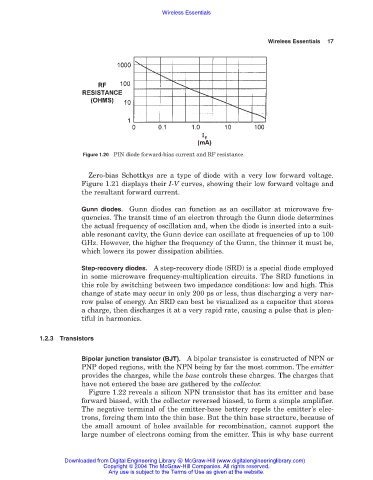
Figure 1.20 PIN diode forward-bias current and RF resistance.
Zero-bias Schottkys are a type of diode with a very low forward voltage.
Figure 1.21 displays their I-V curves, showing their low forward voltage and
the resultant forward current.
Gunn diodes. Gunn diodes can function as an oscillator at microwave fre-
quencies. The transit time of an electron through the Gunn diode determines
the actual frequency of oscillation and, when the diode is inserted into a suit-
able resonant cavity, the Gunn device can oscillate at frequencies of up to 100
GHz. However, the higher the frequency of the Gunn, the thinner it must be,
which lowers its power dissipation abilities.
Step-recovery diodes. A step-recovery diode (SRD) is a special diode employed
in some microwave frequency-multiplication circuits. The SRD functions in
this role by switching between two impedance conditions: low and high. This
change of state may occur in only 200 ps or less, thus discharging a very nar-
row pulse of energy. An SRD can best be visualized as a capacitor that stores
a charge, then discharges it at a very rapid rate, causing a pulse that is plen-
tiful in harmonics.
1.2.3 Transistors
Bipolar junction transistor (BJT). A bipolar transistor is constructed of NPN or
PNP doped regions, with the NPN being by far the most common. The emitter
provides the charges, while the base controls these charges. The charges that
have not entered the base are gathered by the collector.
Figure 1.22 reveals a silicon NPN transistor that has its emitter and base
forward biased, with the collector reversed biased, to form a simple amplifier.
The negative terminal of the emitter-base battery repels the emitter’s elec-
trons, forcing them into the thin base. But the thin base structure, because of
the small amount of holes available for recombination, cannot support the
large number of electrons coming from the emitter. This is why base current
Downloaded from Digital Engineering Library @ McGraw-Hill (www.digitalengineeringlibrary.com)
Copyright © 2004 The McGraw-Hill Companies. All rights reserved.
Any use is subject to the Terms of Use as given at the website.