
Page 20 - Complete Wireless Design
P. 20
Wireless Essentials
Wireless Essentials 19
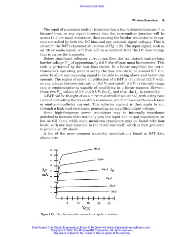
The input of a common-emitter transistor has a low resistance because of its
forward bias, so any signal inserted into the base-emitter junction will be
across this low input resistance, thus causing the bipolar transistor to be cur-
rent controlled by both the DC bias and any external signal voltages. This is
shown in the BJT’s characteristic curves of Fig. 1.23. The input signal, such as
an RF or audio signal, will then add to or subtract from the DC bias voltage
that is across the transistor.
Before significant collector current can flow, the transistor’s emitter-base
barrier voltage V of approximately 0.6 V (for silicon) must be overcome. This
BE
task is performed by the base bias circuit. In a linear amplifier, the initial
transistor’s operating point is set by the bias circuits to be around 0.7 V in
order to allow any incoming signal to be able to swing above and below this
amount. The region of active amplification of a BJT is only about 0.2 V wide,
so any voltage between saturation (0.8 V) and cutoff (0.6 V) is the only range
that a semiconductor is capable of amplifying in a linear manner. Between
these two V values of 0.6 and 0.8 V, the I , and thus the I , is controlled.
BE B C
A BJT can be thought of as a current-controlled resistance, with a tiny base
current controlling the transistor’s resistance, which influences the much larg-
er emitter-to-collector current. This collector current is then made to run
through a high load resistance, generating an amplified output voltage.
Some high-frequency power transistors may be internally impedance
matched to increase their normally very low input and output impedances (as
low as 0.5 ohm), while some metal-can transistors may be found with four
leads; with one lead attached to the metal can itself, which is then grounded
to provide an RF shield.
A few of the more common transistor specifications found in BJT data
sheets are:
Figure 1.23 The characteristic curves for a bipolar transistor.
Downloaded from Digital Engineering Library @ McGraw-Hill (www.digitalengineeringlibrary.com)
Copyright © 2004 The McGraw-Hill Companies. All rights reserved.
Any use is subject to the Terms of Use as given at the website.