
Page 25 - Complete Wireless Design
P. 25
Wireless Essentials
24 Chapter One
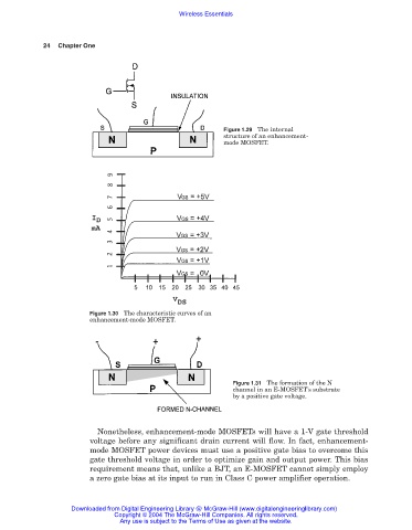
Figure 1.29 The internal
structure of an enhancement-
mode MOSFET.
Figure 1.30 The characteristic curves of an
enhancement-mode MOSFET.
Figure 1.31 The formation of the N
channel in an E-MOSFET’s substrate
by a positive gate voltage.
Nonetheless, enhancement-mode MOSFETs will have a 1-V gate threshold
voltage before any significant drain current will flow. In fact, enhancement-
mode MOSFET power devices must use a positive gate bias to overcome this
gate threshold voltage in order to optimize gain and output power. This bias
requirement means that, unlike a BJT, an E-MOSFET cannot simply employ
a zero gate bias at its input to run in Class C power amplifier operation.
Downloaded from Digital Engineering Library @ McGraw-Hill (www.digitalengineeringlibrary.com)
Copyright © 2004 The McGraw-Hill Companies. All rights reserved.
Any use is subject to the Terms of Use as given at the website.