
Page 206 - Complete Wireless Design
P. 206
Amplifier Design
Amplifier Design 205
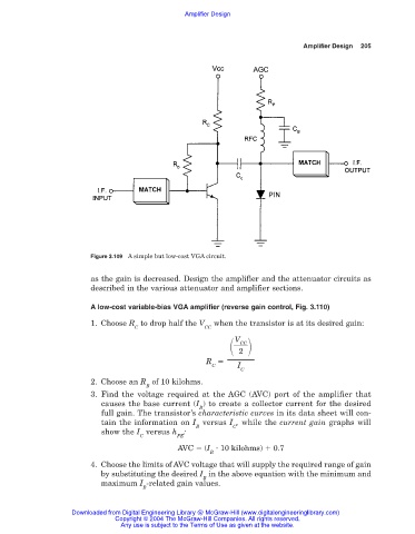
Figure 3.109 A simple but low-cost VGA circuit.
as the gain is decreased. Design the amplifier and the attenuator circuits as
described in the various attenuator and amplifier sections.
A low-cost variable-bias VGA amplifier (reverse gain control, Fig. 3.110)
1. Choose R to drop half the V when the transistor is at its desired gain:
C CC
V
CC
2
R
C I
C
2. Choose an R of 10 kilohms.
B
3. Find the voltage required at the AGC (AVC) port of the amplifier that
causes the base current (I ) to create a collector current for the desired
B
full gain. The transistor’s characteristic curves in its data sheet will con-
tain the information on I versus I , while the current gain graphs will
B C
show the I versus h :
C FE
AVC (I 10 kilohms) 0.7
B
4. Choose the limits of AVC voltage that will supply the required range of gain
by substituting the desired I in the above equation with the minimum and
B
maximum I -related gain values.
B
Downloaded from Digital Engineering Library @ McGraw-Hill (www.digitalengineeringlibrary.com)
Copyright © 2004 The McGraw-Hill Companies. All rights reserved.
Any use is subject to the Terms of Use as given at the website.