
Page 207 - Complete Wireless Design
P. 207
Amplifier Design
206 Chapter Three
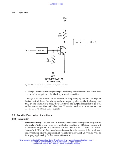
Figure 3.110 A circuit for a variable-bias gain amplifier.
5. Design the transistor’s input/output matching networks for the desired bias
at maximum gain and for the frequency of operation.
The gain of the circuit is now controlled completely by the AGC voltage at
the transistor’s base. But since gain is managed by altering the I through the
C
AGC at the transistor’s base, then the input and output impedances, as well
as the stage’s stability, will also vary. Distortion and gain compression may
also occur with strong input signals.
3.9 Coupling/Decoupling of Amplifiers
3.9.1 Introduction
Amplifier coupling. To prevent DC biasing of consecutive amplifier stages from
adversely affecting other stages, a method of coupling an AC signal into or out
of another amplifier—or another source and its load—must be found.
Unmatched RF amplifiers also demand a good impedance match for maximum
power transfer and the reduction of reflections (decreased VSWR), as well as
for supplying filtering for harmonic attenuation.
Downloaded from Digital Engineering Library @ McGraw-Hill (www.digitalengineeringlibrary.com)
Copyright © 2004 The McGraw-Hill Companies. All rights reserved.
Any use is subject to the Terms of Use as given at the website.