
Page 202 - Complete Wireless Design
P. 202
Amplifier Design
Amplifier Design 201
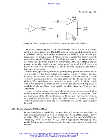
Figure 3.106 The output power of a single MMIC compared to two paralleled MMICs.
As stated, paralleling two MMICs will increase their P1dB by 3 dB as com-
pared to a single device, and Fig. 3.107 shows a recommended circuit for such
a two-MMIC setup. This design maintains the MMICs’ input and output
impedances by using a lumped Wilkinson power divider/combiner network,
along with a single DC bias line. The Wilkinson network, unfortunately, will
also make the amplifiers much more narrowband. And, since MMICs are not
always completely resistive, some tuning out of the small MMIC reactances
may be needed by the tweaking of C and C to peak the gain at the desired
1 6
frequency of operation.
Since directly paralleling discrete high-frequency power transistors makes
their already very low input/output impedances even lower, effective low-loss
matching can become a problem. With these types of discrete designs, it is bet-
ter to first match each active device first, preferably to 100 ohms in a 2 par-
allel amplifier, and then directly combine, as shown in Fig. 3.105. Or, match
each active device to 50 ohms, and then utilize the combiner of Fig. 3.107 to
blend the single amplifiers into a parallel amplifier stage (see “Splitters and
Combiners”).
Formerly, indiscriminant direct paralleling of active devices would lead to
uneven current distribution among the transistors, and the subsequent ther-
mal destruction of the affected transistor with the most current draw. This is
not a problem with the vast majority of modern power transistors because of
emitter ballast resistors that are placed internally within the semiconductor
die itself.
3.6.2 Design of parallel MMIC amplifiers
As mentioned above, paralleling two amplifiers will double the available out-
put power, increasing it by 3 dB. To design the 50-ohm MMIC parallel power
amplifier of Fig. 3.107, bias as instructed in Sec. 3.4.2 under “MMIC Biasing
Procedure,” couple as in Sec. 3.4.3, “MMIC Coupling and Decoupling,” and
use the following power splitter/combiner formulas to design the input/output
network:
Downloaded from Digital Engineering Library @ McGraw-Hill (www.digitalengineeringlibrary.com)
Copyright © 2004 The McGraw-Hill Companies. All rights reserved.
Any use is subject to the Terms of Use as given at the website.