
Page 198 - Complete Wireless Design
P. 198
Amplifier Design
Amplifier Design 197
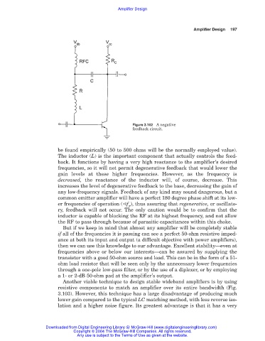
Figure 3.102 A negative
feedback circuit.
be found empirically (50 to 500 ohms will be the normally employed value).
The inductor (L) is the important component that actually controls the feed-
back. It functions by having a very high reactance to the amplifier’s desired
frequencies, so it will not permit degenerative feedback that would lower the
gain levels at these higher frequencies. However, as the frequency is
decreased, the reactance of the inductor will, of course, decrease. This
increases the level of degenerative feedback to the base, decreasing the gain of
any low-frequency signals. Feedback of any kind may sound dangerous, but a
common emitter amplifier will have a perfect 180 degree phase shift at its low-
er frequencies of operation ( f ), thus assuring that regenerative, or oscillato-
T
ry, feedback will not occur. The only caution would be to confirm that the
inductor is capable of blocking the RF at its highest frequency, and not allow
the RF to pass through because of parasitic capacitances within this choke.
But if we keep in mind that almost any amplifier will be completely stable
if all of the frequencies it is passing can see a perfect 50-ohm resistive imped-
ance at both its input and output (a difficult objective with power amplifiers),
then we can use this knowledge to our advantage. Excellent stability—even at
frequencies above or below our interests—can be assured by supplying the
transistor with a good 50-ohm source and load. This can be in the form of a 51-
ohm load resistor that will be seen only by the unnecessary lower frequencies
through a one-pole low-pass filter, or by the use of a diplexer, or by employing
a 1- or 2-dB 50-ohm pad at the amplifier’s output.
Another viable technique to design stable wideband amplifiers is by using
resistive components to match an amplifier over its entire bandwidth (Fig.
3.103). However, this technique has a large disadvantage of producing much
lower gain compared to the typical LC matching method, with less reverse iso-
lation and a higher noise figure. Its greatest advantage is that it has a very
Downloaded from Digital Engineering Library @ McGraw-Hill (www.digitalengineeringlibrary.com)
Copyright © 2004 The McGraw-Hill Companies. All rights reserved.
Any use is subject to the Terms of Use as given at the website.