
Page 194 - Complete Wireless Design
P. 194
Amplifier Design
Amplifier Design 193
will be used in receiver front-end applications. For optimum NF, some simu-
lation runs and tweaking on the prototype board are usually required for any
matching network. Agilent’s recommended L value for 800 MHz is 22 nH,
match
900 MHz is 18 nH, 1.5 GHz is 8.2 nH, 1.9 GHz is 5.6 nH, and 2.4 GHz is 2.7
nH. Above 3 GHz no inductor is required. The RF output of the MGA-85563 is
50 ohms, so no matching network is required at this port. Pin 6 outputs the
RF through the DC blocking capacitor C , while the DC (voltage-based) bias is
C
also injected into pin 6. The RFC blocks the RF from entering V , and the two
CC
capacitors C bypass any RF that makes it through the RFC, while also filter-
B
ing power supply EMI from entering the MMIC. Pin 4 of the MGA-85563 can
be utilized to increase the IP3 at the RF output by increasing the MMIC’s bias
current from its normal 15 mA up to 35 mA. Since this mode obviously con-
sumes more current, it is employed only when higher output powers are
required. With pin 4 left floating, the device will have an IP3 of 12 dBm,
while an R of 15 ohms will cause an I of 30 mA and raise the IP3 to 17 dBm.
b d
3.4.5 MMIC layout
In most MMIC and RFIC layouts, it is normally undesirable to tie all the
ground pins together to a single through-hole via to the ground plane, partic-
ularly if the ground pins are separated by any distance. This is because the
feedback from one internal stage to another creates instabilities within the
MMIC itself. Since most MMICs have at least two internal amplification
stages, direct grounding by the shortest route possible is vitally important to
prevent not only MMIC instability but also undesirable frequency gain peak-
ing, as well as decreased input return loss caused by high impedance ground
loops between these various internal amplifier stages, causing regenerative
feedback. In addition, at microwave frequencies, it is always advisable to use
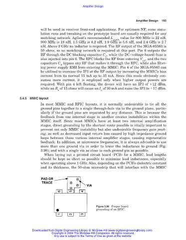
more than one ground via in order to lower the inductance to ground (Fig.
3.98); and with a single via as close to each ground pin as possible.
When laying out a printed circuit board (PCB) for a MMIC, lead lengths
should be kept as short as possible to minimize lead inductance, especially
when operating above 1 GHz. Also, depending on the PCB’s dielectric constant
and its thickness, the 50-ohm microstrip that will interface with the MMIC
Figure 3.98 Proper board
grounding of an RFIC.
Downloaded from Digital Engineering Library @ McGraw-Hill (www.digitalengineeringlibrary.com)
Copyright © 2004 The McGraw-Hill Companies. All rights reserved.
Any use is subject to the Terms of Use as given at the website.