
Page 189 - Complete Wireless Design
P. 189
Amplifier Design
188 Chapter Three
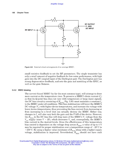
Figure 3.94 Internal circuit arrangement of an average MMIC.
small resistive feedback to set the RF parameters. The single transistor has
only a small amount of negative feedback for low-noise performance, with high
gain into the DC coupled input of the Darlington pair. The Darlington pair has
strong degenerative feedback, and sets the gain and matching of the RFIC, as
well as the gain flatness.
3.4.2 MMIC biasing
The current-biased MMIC (by far the most common type), will attempt to draw
more current as the temperature rises. To preserve a MMIC’s drain current (I )
d
so that its Q-point bias does not vary with temperature or large input signals,
the DC bias circuitry consisting of R , Fig. 3.95) must maintain a constant I
BIAS d
to the MMIC under all conditions. This bias stabilization will lower the MMIC’s
DC voltage (V ) with higher device temperatures, and increase the voltage with
d
lower device temperatures, thus preventing the bias current from decreasing or
from increasing to a level that can actually destroy the MMIC. Either way,
changes in I will also vary both the gain and the P1dB of the device. However,
d
the R in the DC bias line will drop more of the MMIC’s V voltage from the
BIAS d
V supply (since V IR), which decreases V and, consequently, the MMIC’s
CC d
bias current to the desired levels. Since the effectiveness of this temperature
bias control is dependent on the voltage drop across R , a value of up to 4 V
BIAS
may be required for proper stabilization over a temperature range of 25°C to
100°C. By using a higher value resistance of R along with a higher supply
BIAS
voltage, stabilization is improved. Nevertheless, R should not have such
BIAS
Downloaded from Digital Engineering Library @ McGraw-Hill (www.digitalengineeringlibrary.com)
Copyright © 2004 The McGraw-Hill Companies. All rights reserved.
Any use is subject to the Terms of Use as given at the website.