Page 185 - Complete Wireless Design
P. 185

Amplifier Design


            184  Chapter Three


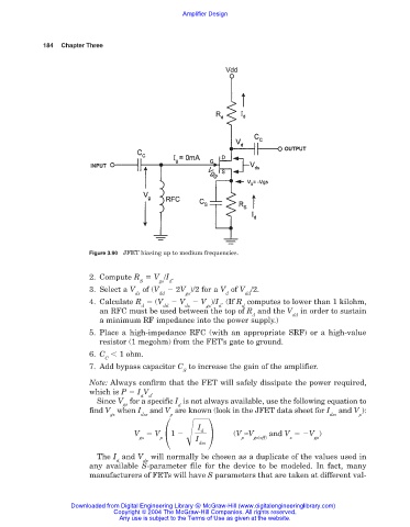
                        Figure 3.90 JFET biasing up to medium frequencies.

                        2. Compute R   V /I .
                                     S    gs  d
                        3. Select a V of (V    2V )/2 for a V of V /2.
                                    ds    dd     gs         d    dd
                        4. Calculate R   (V    V   V )/I . (If R computes to lower than 1 kilohm,
                                      d    dd    ds    gs  d    d
                           an RFC must be used between the top of R and the V  in order to sustain
                                                                   d         dd
                           a minimum RF impedance into the power supply.)
                        5. Place a high-impedance RFC (with an appropriate SRF) or a high-value
                           resistor (1 megohm) from the FET’s gate to ground.
                        6. C   1 ohm.
                            C
                        7. Add bypass capacitor C to increase the gain of the amplifier.
                                                 S
                        Note: Always confirm that the FET will safely dissipate the power required,
                        which is P   I V .
                                      d  d
                          Since V for a specific I is not always available, use the following equation to
                                 gs            d
                        find V when I   and V are known (look in the JFET data sheet for I  and V ):
                              gs      dss    p                                         dss    p

                                                    I
                                                     d
                                    V   V    1                (V ≈V    and V   V )
                                     gs    p        I           p  gs(off)  s      gs
                                                     dss
                          The I and V will normally be chosen as a duplicate of the values used in
                               d      ds
                        any available  S-parameter file for the device to be modeled. In fact, many
                        manufacturers of FETs will have S parameters that are taken at different val-

                   Downloaded from Digital Engineering Library @ McGraw-Hill (www.digitalengineeringlibrary.com)
                               Copyright © 2004 The McGraw-Hill Companies. All rights reserved.
                                Any use is subject to the Terms of Use as given at the website.
   180   181   182   183   184   185   186   187   188   189   190