
Page 184 - Complete Wireless Design
P. 184
Amplifier Design
Amplifier Design 183
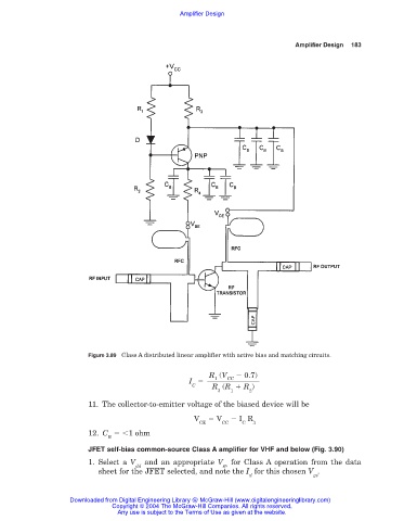
Figure 3.89 Class A distributed linear amplifier with active bias and matching circuits.
R (V 0.7)
CC
1
I
C R (R R )
3 1 2
11. The collector-to-emitter voltage of the biased device will be
V V I R
CE CC C 3
12. C 1 ohm
B
JFET self-bias common-source Class A amplifier for VHF and below (Fig. 3.90)
1. Select a V and an appropriate V for Class A operation from the data
dd gs
sheet for the JFET selected, and note the I for this chosen V .
d gs
Downloaded from Digital Engineering Library @ McGraw-Hill (www.digitalengineeringlibrary.com)
Copyright © 2004 The McGraw-Hill Companies. All rights reserved.
Any use is subject to the Terms of Use as given at the website.