
Page 187 - Complete Wireless Design
P. 187
Amplifier Design
186 Chapter Three
7. Calculate V V V .
g gs s
8. Use an R value of 220 kilohms (this effects the DC input resistance).
1
9. Calculate
R (V V )
g
1
dd
R
2 V
g
Note: The I and V will usually be chosen as a duplicate of the values used in
d ds
any available S-parameter file for the device to be modeled. In fact, many
manufacturers of FETs will have available S parameters taken at different
values of V and I . (I is usually quoted as a percent of I —the maximum
ds d d dss
I —such as “50 percent of I ,” which would work well for Class A bias.)
d dss
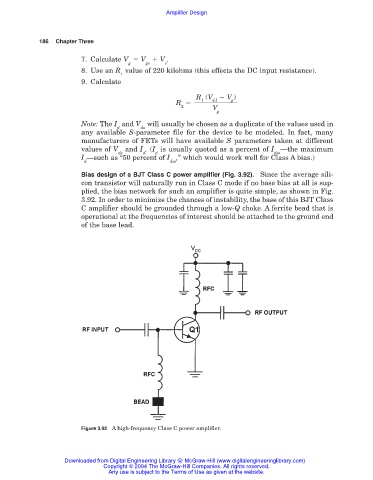
Bias design of a BJT Class C power amplifier (Fig. 3.92). Since the average sili-
con transistor will naturally run in Class C mode if no base bias at all is sup-
plied, the bias network for such an amplifier is quite simple, as shown in Fig.
3.92. In order to minimize the chances of instability, the base of this BJT Class
C amplifier should be grounded through a low-Q choke. A ferrite bead that is
operational at the frequencies of interest should be attached to the ground end
of the base lead.
Figure 3.92 A high-frequency Class C power amplifier.
Downloaded from Digital Engineering Library @ McGraw-Hill (www.digitalengineeringlibrary.com)
Copyright © 2004 The McGraw-Hill Companies. All rights reserved.
Any use is subject to the Terms of Use as given at the website.