
Page 191 - Complete Wireless Design
P. 191
Amplifier Design
190 Chapter Three
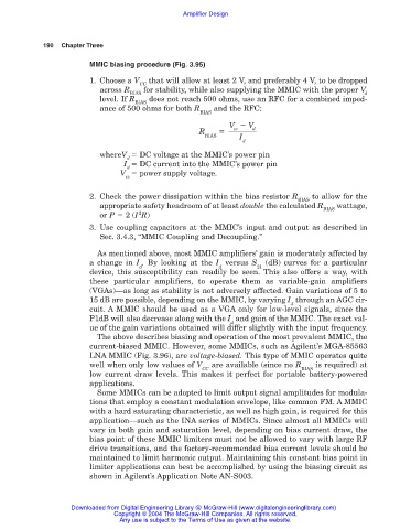
MMIC biasing procedure (Fig. 3.95)
1. Choose a V that will allow at least 2 V, and preferably 4 V, to be dropped
CC
across R for stability, while also supplying the MMIC with the proper V
BIAS d
level. If R does not reach 500 ohms, use an RFC for a combined imped-
BIAS
ance of 500 ohms for both R and the RFC:
BIAS
V V
cc
R d
BIAS I
d
whereV DC voltage at the MMIC’s power pin
d
I DC current into the MMIC’s power pin
d
V power supply voltage.
cc
2. Check the power dissipation within the bias resistor R to allow for the
BIAS
appropriate safety headroom of at least double the calculated R wattage,
BIAS
2
or P 2 (I R)
3. Use coupling capacitors at the MMIC’s input and output as described in
Sec. 3.4.3, “MMIC Coupling and Decoupling.”
As mentioned above, most MMIC amplifiers’ gain is moderately affected by
a change in I . By looking at the I versus S (dB) curves for a particular
d d 21
device, this susceptibility can readily be seen. This also offers a way, with
these particular amplifiers, to operate them as variable-gain amplifiers
(VGAs)—as long as stability is not adversely affected. Gain variations of 5 to
15 dB are possible, depending on the MMIC, by varying I through an AGC cir-
d
cuit. A MMIC should be used as a VGA only for low-level signals, since the
P1dB will also decrease along with the I and gain of the MMIC. The exact val-
d
ue of the gain variations obtained will differ slightly with the input frequency.
The above describes biasing and operation of the most prevalent MMIC, the
current-biased MMIC. However, some MMICs, such as Agilent’s MGA-85563
LNA MMIC (Fig. 3.96), are voltage-biased. This type of MMIC operates quite
well when only low values of V are available (since no R is required) at
CC BIAS
low current draw levels. This makes it perfect for portable battery-powered
applications.
Some MMICs can be adopted to limit output signal amplitudes for modula-
tions that employ a constant modulation envelope, like common FM. A MMIC
with a hard saturating characteristic, as well as high gain, is required for this
application—such as the INA series of MMICs. Since almost all MMICs will
vary in both gain and saturation level, depending on bias current draw, the
bias point of these MMIC limiters must not be allowed to vary with large RF
drive transitions, and the factory-recommended bias current levels should be
maintained to limit harmonic output. Maintaining this constant bias point in
limiter applications can best be accomplished by using the biasing circuit as
shown in Agilent’s Application Note AN-S003.
Downloaded from Digital Engineering Library @ McGraw-Hill (www.digitalengineeringlibrary.com)
Copyright © 2004 The McGraw-Hill Companies. All rights reserved.
Any use is subject to the Terms of Use as given at the website.