
Page 195 - Complete Wireless Design
P. 195
Amplifier Design
194 Chapter Three
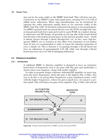
may not be the same width as the MMIC lead itself. This will form step dis-
continuities at the MMIC’s input and output ports, creating 0.01 to 0.2 nH of
added series inductance. These step discontinuities can be minimized by
tapering the wider microstrip rapidly down to the narrower width of the
MMIC lead (Fig. 3.99). To minimize undesired inductance to the ground plane,
the MMIC’s ground leads are placed directly over the PCB’s through-hole vias,
as long ground leads lower gain and result in a poor P1dB. As a matter of prop-
er microwave and RF design, all grounds on the top side of the board should
lead directly to the bottom ground plane by the shortest possible route—which
is almost always through a direct through-hole via. In fact, some high-fre-
quency MMICs are so sensitive to this effect that substrates of not thicker
than 32 mils are recommended in order to lessen the inductive properties of
even a simple via. This is because a via passing through a 32-mil board can
have an inductance of approximately 0.15 nH, while vias through a 62-mil
board may have up to 0.5 nH of damaging inductance.
3.5 Wideband Amplifiers
3.5.1 Introduction
A wideband MMIC or discrete amplifier is designed to have an extremely
broad band of frequencies that it can pass with flat gain and (preferably) a
decent return loss response—along with perfect stability.
In order to properly design a discrete wideband RF amplifier we must sup-
press the lower frequencies, where the gain is the highest (Fig. 3.100a). One
way to do this is by giving these frequencies a poor impedance match, while
with the higher frequencies—where the gain is much less—we can give a per-
fect match. This will flatten the gain of the amplifier (Fig. 3.100b), but will not
Figure 3.99 Proper board layout for an MMIC as seen from top of PCB.
Downloaded from Digital Engineering Library @ McGraw-Hill (www.digitalengineeringlibrary.com)
Copyright © 2004 The McGraw-Hill Companies. All rights reserved.
Any use is subject to the Terms of Use as given at the website.