
Page 179 - Complete Wireless Design
P. 179
Amplifier Design
178 Chapter Three
5. X X 1 ohm
CB CC
Alternatively:
1. Select a V of V /2 and an I that is shown by the data sheets to be at a
CE CC C
maximum gain, NF, or P1dB. Or choose a V and an I that are the same
CE C
as in the S-parameter file available for the active device. (Do not confuse
V in S-parameter calculations with V . V can be as high as desired, but
CE CC CC
V must be as stated in the S-parameter file available for the chosen device
CE
for accurate design or simulations.)
V V
CC
CE
2. Calculate R
C I
C
V
0.6
CE
3. Calculate R ß
F I
C
4. X X 1 ohm
CB CC
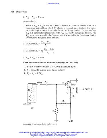
Class A common-collector buffer amplifier (Figs. 3.83 and 3.84):
1. Do not overdrive buffer: 0.3 V RMS maximum input.
2. I ≈ 5 mA (10 mA for more-linear output)
e
3. V V 0.5V
e ce CC
Figure 3.83 A common-collector buffer circuit.
Downloaded from Digital Engineering Library @ McGraw-Hill (www.digitalengineeringlibrary.com)
Copyright © 2004 The McGraw-Hill Companies. All rights reserved.
Any use is subject to the Terms of Use as given at the website.