
Page 174 - Complete Wireless Design
P. 174
Amplifier Design
Amplifier Design 173
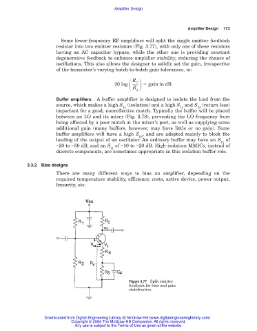
Some lower-frequency RF amplifiers will split the single emitter feedback
resistor into two emitter resistors (Fig. 3.77), with only one of these resistors
having an AC capacitor bypass, while the other one is providing constant
degenerative feedback to enhance amplifier stability, reducing the chance of
oscillations. This also allows the designer to solidly set the gain, irrespective
of the transistor’s varying batch-to-batch gain tolerances, to:
R
C
20 log gain in dB
R
4
Buffer amplifiers. A buffer amplifier is designed to isolate the load from the
source, which makes a high S (isolation) and a high S and S (return loss)
12 11 22
important for a good, nonreflective match. Typically the buffer will be placed
between an LO and its mixer (Fig. 3.78), preventing the LO frequency from
being affected by a poor match at the mixer’s port, as well as supplying some
additional gain (many buffers, however, may have little or no gain). Some
buffer amplifiers will have a high Z , and are adopted mainly to block the
IN
loading of the output of an oscillator. An ordinary buffer may have an S of
12
–20 to –50 dB, and an S of –10 to –20 dB. High-isolation MMICs, instead of
11
discrete components, are sometimes appropriate in this isolation buffer role.
3.3.2 Bias designs
There are many different ways to bias an amplifier, depending on the
required temperature stability, efficiency, costs, active device, power output,
linearity, etc.
Figure 3.77 Split emitter
feedback for bias and gain
stabilization.
Downloaded from Digital Engineering Library @ McGraw-Hill (www.digitalengineeringlibrary.com)
Copyright © 2004 The McGraw-Hill Companies. All rights reserved.
Any use is subject to the Terms of Use as given at the website.