
Page 171 - Complete Wireless Design
P. 171
Amplifier Design
170 Chapter Three
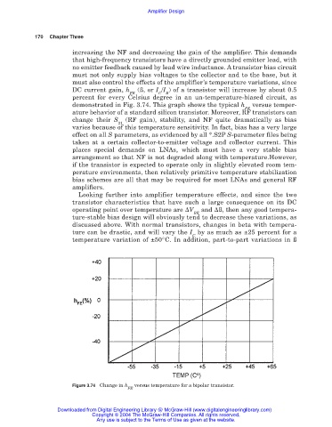
increasing the NF and decreasing the gain of the amplifier. This demands
that high-frequency transistors have a directly grounded emitter lead, with
no emitter feedback caused by lead wire inductance. A transistor bias circuit
must not only supply bias voltages to the collector and to the base, but it
must also control the effects of the amplifier’s temperature variations, since
DC current gain, h (ß, or I /I ) of a transistor will increase by about 0.5
FE C B
percent for every Celsius degree in an un-temperature-biased circuit, as
demonstrated in Fig. 3.74. This graph shows the typical h versus temper-
FE
ature behavior of a standard silicon transistor. Moreover, RF transistors can
change their S (RF gain), stability, and NF quite dramatically as bias
21
varies because of this temperature sensitivity. In fact, bias has a very large
effect on all S parameters, as evidenced by all *.S2P S-parameter files being
taken at a certain collector-to-emitter voltage and collector current. This
places special demands on LNAs, which must have a very stable bias
arrangement so that NF is not degraded along with temperature.However,
if the transistor is expected to operate only in slightly elevated room tem-
perature environments, then relatively primitive temperature stabilization
bias schemes are all that may be required for most LNAs and general RF
amplifiers.
Looking further into amplifier temperature effects, and since the two
transistor characteristics that have such a large consequence on its DC
operating point over temperature are V and ß, then any good tempera-
BE
ture-stable bias design will obviously tend to decrease these variations, as
discussed above. With normal transistors, changes in beta with tempera-
ture can be drastic, and will vary the I by as much as ±25 percent for a
C
temperature variation of ±50°C. In addition, part-to-part variations in ß
Figure 3.74 Change in h versus temperature for a bipolar transistor.
FE
Downloaded from Digital Engineering Library @ McGraw-Hill (www.digitalengineeringlibrary.com)
Copyright © 2004 The McGraw-Hill Companies. All rights reserved.
Any use is subject to the Terms of Use as given at the website.