
Page 168 - Complete Wireless Design
P. 168
Amplifier Design
Amplifier Design 167
a signal with a high amplitude to overcome the reverse or complete lack of bias
at the Class C amplifier’s input.
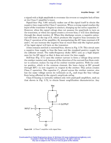
Signal-bias (Fig. 3.69) actually makes use of the signal itself to obtain the
negative bias required for Class C operation. When a strong signal reaches the
input of the transistor it begins to conduct, charging up the series capacitor, C.
However, when the signal voltage does not possess the amplitude to turn on
the transistor, or when the signal creates a reverse bias, C will then discharge
through the shunt resistor, R. When this discharge occurs, a negative poten-
tial will form at the top of R, which produces the negative bias necessary for
Class C operation of the amplifier. By manipulating the RC time constant of R
and C, we can increase the negative bias so much that only the highest peaks
of the input signal will turn on the transistor.
A less common method is external-bias, shown in Fig. 3.70. This circuit uses
a negative bias supply to bias the base and the standard positive supply for
the collector circuit. The radio-frequency choke (RFC) acts as a high imped-
ance for the RF signal so that it does not enter the bias supply.
Self-bias (Fig. 3.71) uses the emitter current to form a voltage drop across
the emitter resistor and, because of the direction of the current flow from emit-
ter to collector, makes the top of the emitter resistor positive. With the emit-
ter positive, which is the common element, the base—being at DC ground
through RFC—is now negative in respect to the emitter. This action creates
Class C operation. The capacitor C , placed across the emitter resistor, also
E
has the same voltage across its terminals as R , and stops the bias voltage
E
from being affected by the signal’s amplitude swing.
Class B biasing is normally utilized only with push-pull amplifiers, such as
that shown in Fig. 3.72, to obtain linear amplification characteristics. Any
Figure 3.69 A Class C amplifier with signal bias.
Downloaded from Digital Engineering Library @ McGraw-Hill (www.digitalengineeringlibrary.com)
Copyright © 2004 The McGraw-Hill Companies. All rights reserved.
Any use is subject to the Terms of Use as given at the website.