
Page 163 - Complete Wireless Design
P. 163
Amplifier Design
162 Chapter Three
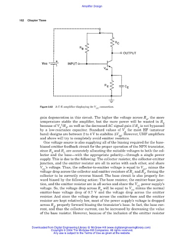
Figure 3.62 A C-E amplifier displaying its V connection.
CC
gain degeneration in this circuit. The higher the voltage across R , the more
E
temperature stable the amplifier, but the more power will be wasted in R
E
2
because of V /R , as well as the decreased AC signal gain if R is not bypassed
E E E
by a low-reactance capacitor. Standard values of V for most HF (amateur
E
band) designs are between 2 to 4 V to stabilize V . However, UHF amplifiers
BE
and above will try to completely avoid emitter resistors.
One voltage source is also supplying all of the biasing required for the base-
biased emitter feedback circuit for the proper operation of the NPN transistor,
since R and R are accurately allocating the suitable voltages to both the col-
B C
lector and the base—with the appropriate polarity—through a single power
supply. This is due to the following: The collector resistor, the collector-emitter
junction, and the emitter resistor are all in series with each other, and share
V ’s voltage. Thus, the collector-to-emitter voltage is equal to V , minus the
CC CC
voltage drop across the collector and emitter resistors of R and R , forcing the
C E
collector to be correctly reverse biased. The base circuit is also properly for-
ward biased by the following action: The base resistor, the emitter-base junc-
tion, and the emitter resistor are in all series and share the V power supply’s
CC
voltage. So, the voltage drop across R will be equal to V minus the normal
B CC
emitter-base voltage drop of 0.7 V and the voltage drop across the emitter
resistor. And since the voltage drop across the emitter-base and the emitter
resistor are kept relatively low, most of the power supply’s voltage is dropped
across R , properly forward biasing the transistor’s base. In fact, the base cur-
B
rent, and thus the collector current, can be increased by decreasing the value
of the base resistor. However, because of the inclusion of the emitter resistor
Downloaded from Digital Engineering Library @ McGraw-Hill (www.digitalengineeringlibrary.com)
Copyright © 2004 The McGraw-Hill Companies. All rights reserved.
Any use is subject to the Terms of Use as given at the website.