
Page 166 - Complete Wireless Design
P. 166
Amplifier Design
Amplifier Design 165
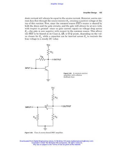
drain current will always be equal to the source current. However, source cur-
rent does flow through the source resistor R , creating a positive voltage at the
S
top of this resistor. Now, since the common-source FET’s source is shared by
both the drain and the gate circuits, and the gate will always be at zero volts
with respect to ground—since no gate current equals no voltage drop across
R —the gate is now negative with respect to the common source. This allows
G
the FET to be biased at its Class A, AB, or B Q points, depending on the val-
ue chosen for R , while a capacitor can be inserted across R to restrain the
S S
bias voltage to a steady DC value.
Figure 3.65 A common-emitter
amplifier with collector
feedback bias.
Figure 3.66 Class A source-biased FET amplifier.
Downloaded from Digital Engineering Library @ McGraw-Hill (www.digitalengineeringlibrary.com)
Copyright © 2004 The McGraw-Hill Companies. All rights reserved.
Any use is subject to the Terms of Use as given at the website.