
Page 162 - Complete Wireless Design
P. 162
Amplifier Design
Amplifier Design 161
applications, but biasing was invented so that these separate voltages could be
obtained from a single supply. Second, transistors are remarkably tempera-
ture sensitive, inviting a condition called thermal runaway. Thermal runaway
will rapidly destroy a bipolar transistor, since collector current quickly and
uncontrollably increases to damaging levels as the temperature rises; unless
the amplifier is temperature stabilized to nullify this effect.
The dominant biasing schemes to obtain both temperature stabilization and
single-supply operation are base-biased emitter feedback, voltage-divider emit-
ter feedback, collector feedback, diode feedback, and active bias. All five are
found in Class A and AB operation, while Class B and C amplifiers can imple-
ment other methods. Which bias circuit to adopt depends on the desired cir-
cuit costs, complexity, stability, and other considerations.
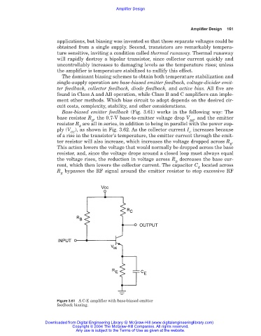
Base-biased emitter feedback (Fig. 3.61) works in the following way: The
base resistor R , the 0.7-V base-to-emitter voltage drop V , and the emitter
B BE
resistor R are all in series, in addition to being in parallel with the power sup-
E
ply (V ), as shown in Fig. 3.62. As the collector current I increases because
CC C
of a rise in the transistor’s temperature, the emitter current through the emit-
ter resistor will also increase, which increases the voltage dropped across R .
E
This action lowers the voltage that would normally be dropped across the base
resistor, and, since the voltage drops around a closed loop must always equal
the voltage rises, the reduction in voltage across R decreases the base cur-
B
rent, which then lowers the collector current. The capacitor C located across
E
R bypasses the RF signal around the emitter resistor to stop excessive RF
E
Figure 3.61 A C-E amplifier with base-biased emitter
feedback biasing.
Downloaded from Digital Engineering Library @ McGraw-Hill (www.digitalengineeringlibrary.com)
Copyright © 2004 The McGraw-Hill Companies. All rights reserved.
Any use is subject to the Terms of Use as given at the website.