
Page 158 - Complete Wireless Design
P. 158
Amplifier Design
Amplifier Design 157
under almost any adverse load condition (any power amplifier must, especial-
ly in today’s competitive market, not self-destruct in a short- or open-circuited
state). In addition, if the power transistor has appropriate heat sinking, the
amplifier will have a much stronger chance of withstanding very poor return
losses caused by a missing or short-circuited load.
In order to minimize the chances of instability, the base of a power BJT Class
C amplifier should be grounded through a low-Q choke (Fig. 3.53), with a fer-
rite bead that is operational at these frequencies attached to the grounded end
of the base lead. Decreasing low-frequency gain, which is naturally at an
increased level, will also assist in stability. This is discussed under “Gain flat-
tening,” below. And the proper RF grounding of the transistor’s emitter leads
will help in maintaining gain and avoiding oscillations, since the smallest
amount of inductance in this path to ground can prove disastrous to a power
transistor. In fact, even the naturally occurring parasitic inductances and
capacitances in the passive elements used for biasing, coupling, and decoupling
should be modeled in software to prevent unnecessary and expensive tweaking
of the completed power amplifier.
Gain flattening. All wideband power amplifiers should incorporate some type
of compensation to maintain a flat gain across their entire bandwidth to with-
in 2 dB or better. This is needed because of an amplifier’s inclination to pos-
sess a higher gain at its lower frequencies than at its higher frequencies; gain
decreases at 6 dB per octave as frequency increases. The high gain, as men-
tioned above, can cause low-frequency instabilities and subsequent transistor
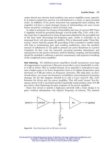
damage. By far the simplest method is to add a losser network (Fig. 3.55)
between the driver and the power amplifier. This will send “excess” low-fre-
quency power to R at an almost perfect amplitude compensation value of 6 dB
per octave, thus flattening the gain response of the power amplifier.
Since this circuit is merely a high-pass network with a load, design it to
pass—without attenuation—the highest frequency of interest. The natural
Figure 3.55 Gain flattening with an LR losser network.
Downloaded from Digital Engineering Library @ McGraw-Hill (www.digitalengineeringlibrary.com)
Copyright © 2004 The McGraw-Hill Companies. All rights reserved.
Any use is subject to the Terms of Use as given at the website.