Page 153 - Complete Wireless Design
P. 153
Amplifier Design


            152  Chapter Three

                        representation, or in a much easier to read tabular format on the device’s data
                        sheet. If desired, the series impedance values can be converted to a shunt
                        impedance (as presented earlier in this chapter), if this information is not so
                        provided. When provided, they may be in the form of a separate graph of input
                        and output parallel equivalent  resistance versus frequency, and a graph of
                        input and output parallel equivalent capacitance versus frequency, at a set V
                                                                                              CC
                        and P   .
                              OUT
                          Designing Class C power amplifiers with small-signal  S parameters will
                        result in a circuit that is not optimized and will not function as intended. This
                        is because any transistor’s input resistance, capacitance, gain, and output
                        resistance will be significantly different when the device is run as a large-sig-
                        nal power amplifier as opposed to a small-signal, Class A amplifier. However,
                        sometimes S parameters may be placed on power MOSFET data sheets, but
                        are only to be utilized to approximate a beginning design, which must then be
                        tweaked in software, and then hardware.
                          Impedance matching, especially in RF power amplifiers, is required so that
                        the transfer of energy to the next stage is accomplished with as little wasted
                        power as possible. Matching that increases the return loss (decreasing the
                        VSWR) of a system or amplifier prevents ripples in the passband of filters
                        from forming and permits the active device to perform as designed with a flat
                        gain, proper NF, low distortion, and high stability.
                          Since the input and output impedances of a power transistor are a complex
                        impedance (Fig. 3.52), and this input impedance can be at very low values
                        (which can necessitate an impedance transformation ratio of up to 20 times for
                        a BJT), it can be seen that proper matching of a power amplifier to its source
                        and load is anything but trivial. And the higher the desired output power of
                        the large-signal transistor, the lower will be its output impedance, which can
                        make matching difficult, especially at these high power levels. In fact, the
                        design of power amplifiers just a few short years ago involved much trial and
                        error in the tweaking of matching and bias networks in order to obtain an effi-
                        cient and workable amplifier that did not self-destruct and had viable compo-
                        nent values. To a lesser extent, this is still the case, but usually only in order
                        to fine-tune the amplifier for low VSWR, high gain, maximum efficiency, and
                        maximum output power because of real-world component tolerances as well as
                        the effects of stray reactances on the completed circuit.
                          The transistor’s input and output impedances will also decrease with an
                        increase in frequency, which further complicates the design of matching net-
                        works for high power amplifiers—especially since these impedances can go
                                1
                        down to    ohm or less.
                                 2
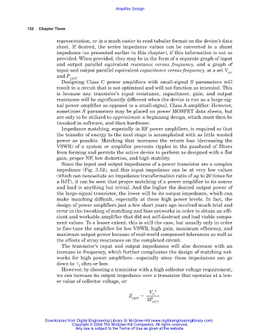
                          However, by choosing a transistor with a high collector voltage requirement,
                        we can increase its output impedance over a transistor that operates at a low-
                        er value of collector voltage, or:
                                                              V  2
                                                                C
                                                      Z
                                                       OUT   2P
                                                               OUT

                   Downloaded from Digital Engineering Library @ McGraw-Hill (www.digitalengineeringlibrary.com)
                               Copyright © 2004 The McGraw-Hill Companies. All rights reserved.
                                Any use is subject to the Terms of Use as given at the website.

