Page 148 - Complete Wireless Design
P. 148

Amplifier Design


                                                                               Amplifier Design  147


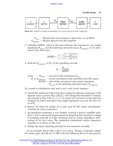
                        Figure 3.48 Selective output mismatching of an active device to lower stage gain.


                                  G      dB gain from the transistor’s data sheet, or use MAG
                                   MAX
                               G         dB gain desired from the amplifier
                                DESIRED
                        3. Calculate RATIO, which is the ratio between the transistor’s real output
                           impedance R      and the matching network’s input, R      (to be calcu-
                                       Q(OUT)                                 IN(MATCH)
                           lated in the next step):


                                                                      M L /10
                                                        1    1   (10  )
                                              RATIO


                                                                      M L /10
                                                        1    1   (10  )
                        4. Find the R       (or R ) of the matching network:
                                     IN(MATCH)   v
                                                            R
                                                             Q (OUT)
                                                      R
                                                        v   RATIO
                           where      R        real part of the transistor’s Z
                                        Q(OUT)                            OUT
                               R or R          virtual resistance at the matching network’s input
                                v    IN(MATCH)
                                      RATIO   ratio of the transistor’s real output impedance
                                               R      to the matching network’s input, R
                                                 Q(OUT)                               IN(MATCH)
                        (R is used in calculations only, and is not a real circuit element.)
                          v
                        5. Cancel the reactance of the transistor’s output by placing a reactance of the
                           opposite value in series (Fig. 3.49; X ). Now design the transistor’s T match-
                                                            L
                           ing network of Fig. 3.50 (L , L , C ) to cancel all reactances in the load, but
                                                    1  2  1
                           designed as if the transistor’s true output impedance was now the new val-
                           ue of R .
                                  v
                        6. Remove  R from the design (it is only used for the initial calculations).
                                     v
                           Combine all series reactances.
                        7. An impedance mismatch is now formed, creating a drop in amplifier gain.
                           This is due to mismatch losses caused by designing the transistor’s output
                           T matching network as if the transistor had an output impedance of R ,
                                                                                               v
                           instead of its true value. The completed mismatched output impedance
                           amplifier is as shown in Fig. 3.51.
                        8. Design the input matching network for the transistor normally.

                          As an example, follow Figs. 3.48 to 3.51 above. Design a transistor ampli-
                        fier with a gain of 6 dB at 1.5 GHz with the following device S parameters:

                   Downloaded from Digital Engineering Library @ McGraw-Hill (www.digitalengineeringlibrary.com)
                               Copyright © 2004 The McGraw-Hill Companies. All rights reserved.
                                Any use is subject to the Terms of Use as given at the website.
   143   144   145   146   147   148   149   150   151   152   153