
Page 150 - Complete Wireless Design
P. 150
Amplifier Design
Amplifier Design 149
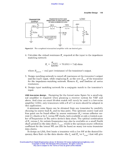
Figure 3.51 The completed mismatched amplifier with our desired gain.
4. Calculate the virtual resistance R required at the input to the impedance
v
matching network:
R
Q(OUT)
R 70.5/9.5 7.42 ohms
v RATIO
where R real part (resistance) of the transistor’s output.
Q(OUT)
5. Design matching network to cancel all reactances at the transistor’s output
and the load’s input, while employing R as the new Z of the transistor
v OUT
for the impedance-matching network. Remove R , and combine all series
v
reactances.
6. Design input matching network for a conjugate match to the transistor’s
input.
LNA low-noise design. Designing for the lowest noise figure for a small-sig-
nal amplifier is required when planning a receiver system for VHF and
above. And since an exact 50-ohm match will rarely be used in a low-noise
amplifier (LNA), only transistors with a K of 1 or more should be adopted in
this application.
A minimum noise figure can be obtained from any transistor by carefully
choosing its source load R and its bias point. This optimum source load and
S
bias point can be found either by source resistance (R ) versus collector cur-
S
rent (I ) charts or by I versus NF charts, both available at only a limited num-
C C
ber of frequencies on the active device’s data sheet. The optimal combination
of R versus I for certain frequencies may also be available on a small Smith
S C
chart printed on the data sheet. , which is the optimum source reflection
S(opt)
coefficient for the lowest NF, can also be found on many low-noise transistor
data sheets.
To design an LNA, first locate a transistor with a low NF at the desired fre-
quency, then find—in the data sheets—the I and R (or ) that will give
C S S(opt)
Downloaded from Digital Engineering Library @ McGraw-Hill (www.digitalengineeringlibrary.com)
Copyright © 2004 The McGraw-Hill Companies. All rights reserved.
Any use is subject to the Terms of Use as given at the website.