Page 151 - Complete Wireless Design
P. 151
Amplifier Design


            150  Chapter Three

                        the best NF. Now design the bias network to supply the chosen I , while the
                                                                                     C
                        optimal source impedance of R is matched at the transistor’s input instead of
                                                     S
                        the true impedance of the source. In other words, if we match the low-noise
                        active device to    by making the LNA “see,” for instance, the antenna’s 50-
                                        S(opt)
                        ohm output impedance as this       value, we can make the LNA transistor
                                                       S(opt)
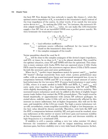
                        supply a low NF (but at an increased VSWR over a perfect power match). We
                        then terminate the transistor’s output by:
                                                 L    S   S S      S(opt)
                                                                21
                                                             12

                                                       22
                                                        1  (S
                                                              11  S(opt) )
                        where        load reflection coefficient
                                  L
                                      optimum source reflection coefficient for the lowest NF (as
                                S(opt)
                                       found on the transistor’s data sheet).

  the complex conjugate of the result
                        Vector quantities should be used for S.
                               will be close to the complex conjugate of the device’s input impedance,
                           S(opt)
                        and will, at times, be so close to S  as to be almost identical. This would be
                                                        11
                        the optimal situation, since NF and VSWR will then be optimized. This situa-
                        tion is more common with GaAs FETs that are operated above 2 GHz (GaAs
                        FETs must be employed in the microwave regions above 2 GHz if BJTs cannot
                        furnish the necessary gain and noise performance).
                          When the S
  (perfect input impedance match for power) and    (perfect
                                     11                                              S(opt)
                        NF “match”) diverge excessively from each other, system performance may
                        suffer, with an associated noise figure and increased mismatch loss. A way to
                        compromise between VSWR and NF is to employ a small amount of source
                        lead inductance for the low-noise FET. If source lead inductance is used under
                        2 GHz, where it is most needed in both FETs and BJTs, S
  and      will
                                                                                11       S(opt)
                        come quite close together, thus hopefully decreasing both NF and VSWR,
                        while slightly decreasing gain—with minimal impact on device stability. This
                        increased source inductance need only be added in the form of slightly longer
                        source leads (before they contact the PCB’s ground plane). The length must be
                        found empirically, or approximated with certain RF software packages. As
                        stated above, stability under 2 GHz will not be dramatically affected by this
                        increase in source inductance, but at higher frequencies, this will not be the
                        case, and instability of the LNA can result. Too high a source inductance val-
                        ue will, nevertheless, create amplifier instability at high or low frequencies, so
                        the best value should be chosen carefully. Therefore, with both the BJT and
                        the FET, a compromise between stability, NF, and gain must be reached, since
                        any inductance at the emitter or source will lower gain and increase stability
                        at low frequencies, but will actually increase gain and decrease stability at
                        high frequencies in a wideband LNA.
                          If stability is still a concern, adding a very low value resistor (13 ohms)
                        between the transistor’s collector and its output matching network will
                        decrease gain, but force stability over a very wide band of frequencies. In fact,


                   Downloaded from Digital Engineering Library @ McGraw-Hill (www.digitalengineeringlibrary.com)
                               Copyright © 2004 The McGraw-Hill Companies. All rights reserved.
                                Any use is subject to the Terms of Use as given at the website.

