
Page 149 - Complete Wireless Design
P. 149
Amplifier Design
148 Chapter Three
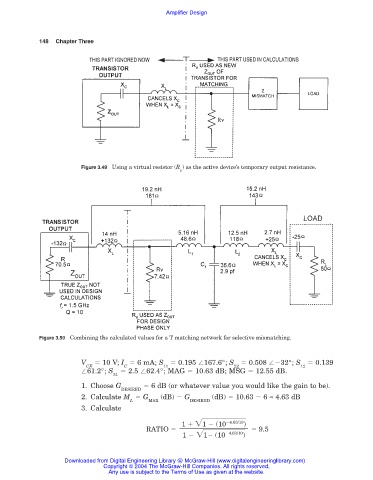
Figure 3.49 Using a virtual resistor (R ) as the active device’s temporary output resistance.
v
Figure 3.50 Combining the calculated values for a T matching network for selective mismatching.
V 10 V; I 6 mA; S 0.195 167.6°; S 0.508 32°; S 0.139
CE C 11 22 12
61.2°; S 2.5 62.4°; MAG 10.63 dB; MSG 12.55 dB.
21
1. Choose G 6 dB (or whatever value you would like the gain to be).
DESIRED
2. Calculate M G (dB) G (dB) 10.63 6 ≈ 4.63 dB
L MAX DESIRED
3. Calculate
4.63/10
1 1 (10 )
RATIO 9.5
4.63/10
1 1 (10 )
Downloaded from Digital Engineering Library @ McGraw-Hill (www.digitalengineeringlibrary.com)
Copyright © 2004 The McGraw-Hill Companies. All rights reserved.
Any use is subject to the Terms of Use as given at the website.