
Page 154 - Complete Wireless Design
P. 154
Amplifier Design
Amplifier Design 153
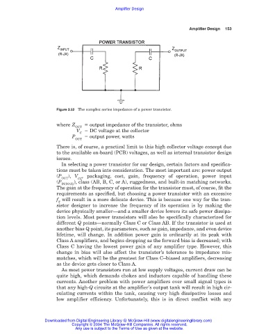
Figure 3.52 The complex series impedance of a power transistor.
where Z output impedance of the transistor, ohms
OUT
V DC voltage at the collector
C
P output power, watts
OUT
There is, of course, a practical limit to this high collector voltage concept due
to the available on-board (PCB) voltages, as well as internal transistor design
issues.
In selecting a power transistor for our design, certain factors and specifica-
tions must be taken into consideration. The most important are: power output
(P ), V , packaging, cost, gain, frequency of operation, power input
OUT CC
(P ), class (AB, B, C, or A), ruggedness, and built-in matching networks.
IN(MAX)
The gain at the frequency of operation for the transistor must, of course, fit the
requirements as specified, but choosing a power transistor with an excessive
f will result in a more delicate device. This is because one way for the tran-
T
sistor designer to increase the frequency of its operation is by making the
device physically smaller—and a smaller device lowers its safe power dissipa-
tion levels. Most power transistors will also be specifically characterized for
different Q points—normally Class C or Class AB. If the transistor is used at
another bias Q point, its parameters, such as gain, impedance, and even device
lifetime, will change. In addition power gain is ordinarily at its peak with
Class A amplifiers, and begins dropping as the forward bias is decreased; with
Class C having the lowest power gain of any amplifier type. However, this
change in bias will also affect the transistor’s tolerance to impedance mis-
matches, which will be the greatest for Class C–biased amplifiers, decreasing
as the device gets closer to Class A.
As most power transistors run at low supply voltages, current draw can be
quite high, which demands chokes and inductors capable of handling these
currents. Another problem with power amplifiers over small signal types is
that any high-Q circuits at the amplifier’s output tank will result in high cir-
culating currents within the tank, causing very high dissipative losses and
low amplifier efficiency. Unfortunately, this is in direct conflict with any
Downloaded from Digital Engineering Library @ McGraw-Hill (www.digitalengineeringlibrary.com)
Copyright © 2004 The McGraw-Hill Companies. All rights reserved.
Any use is subject to the Terms of Use as given at the website.