
Page 156 - Complete Wireless Design
P. 156
Amplifier Design
Amplifier Design 155
3.2.2 Amplifier design with large-signal series equivalent
impedances
The dominant procedure for design of high-power, nonlinear amplifiers is the
large-signal series equivalent impedance method, which characterizes a Class
C, common-emitter power transistor’s equivalent input and output impedances
(Fig. 3.52). The large-signal series equivalent impedance is found in the data
sheet of the power device, and merely represents the complex conjugate, at a
specific V , frequency, power output, power input, and bias where the transis-
CC
tor will supply maximum gain. This does not, however, guarantee that maxi-
mum efficiency will result from such a match, since in wideband amplifier design
the lower frequencies—where gain is naturally at its highest level—may be
purposefully mismatched; while the higher frequencies will be conjugately
matched to peak their gain.
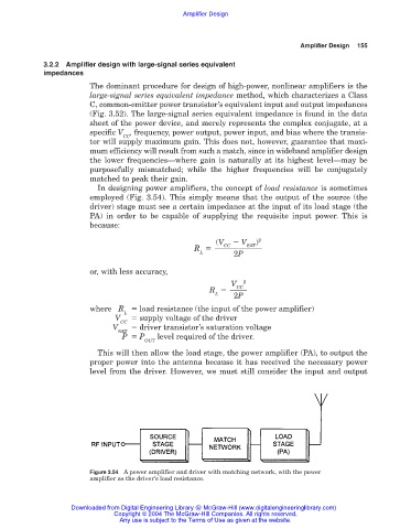
In designing power amplifiers, the concept of load resistance is sometimes
employed (Fig. 3.54). This simply means that the output of the source (the
driver) stage must see a certain impedance at the input of its load stage (the
PA) in order to be capable of supplying the requisite input power. This is
because:
(V V ) 2
SAT
CC
R
L 2P
or, with less accuracy,
V 2
CC
R
L 2P
where R load resistance (the input of the power amplifier)
L
V supply voltage of the driver
CC
V driver transistor’s saturation voltage
SAT
P P level required of the driver.
OUT
This will then allow the load stage, the power amplifier (PA), to output the
proper power into the antenna because it has received the necessary power
level from the driver. However, we must still consider the input and output
Figure 3.54 A power amplifier and driver with matching network, with the power
amplifier as the driver’s load resistance.
Downloaded from Digital Engineering Library @ McGraw-Hill (www.digitalengineeringlibrary.com)
Copyright © 2004 The McGraw-Hill Companies. All rights reserved.
Any use is subject to the Terms of Use as given at the website.