
Page 160 - Complete Wireless Design
P. 160
Amplifier Design
Amplifier Design 159
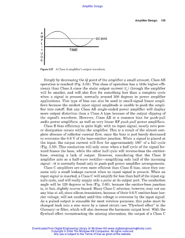
Figure 3.57 A Class A amplifier’s output waveform.
Simply by decreasing the Q point of the amplifier a small amount, Class AB
operation is reached (Fig. 3.58). This class of operation has a little higher effi-
ciency than Class A since the static output current (I ) through the amplifier
C
will be smaller, and will also flow for something less than a complete cycle
when a signal is present, normally around 300 degrees in power amplifier
applications. This type of bias can also be used in small-signal linear ampli-
fiers because the modest input signal amplitude is unable to push the ampli-
fier into cutoff. But any Class AB single-ended power amplifier will display
more output distortion than a Class A type because of the output clipping of
the signal’s waveform. However, Class AB is a common bias for push-pull
audio power amplifiers, as well as very linear RF push-pull power amplifiers.
Class B bias efficiency is quite high: with no input signal, nearly zero pow-
er dissipation occurs within the amplifier. This is a result of the almost com-
plete absence of collector current flow, since the bias is just barely decreased
to overcome the 0.6 V of the base-emitter junction. When a signal is placed at
the input, the output current will flow for approximately 180° of a full cycle
(Fig. 3.59). This conduction will only occur when a half cycle of the signal for-
ward biases the base, while the other half cycle will reverse-bias the emitter-
base, creating a lack of output. However, considering that the Class B
amplifier acts as a half-wave rectifier—amplifying only half of the incoming
signal—it is normally found only in push-pull power amplifier arrangements.
Class C amplifiers are even more efficient than Class B bias, since they con-
sume only a small leakage current when no input signal is present. When an
input signal is inserted, a Class C will amplify for less than half of the input sig-
nal’s cycle, and will really supply only a pulse at its output port. The conduction
angle will be 120 degrees or less (Fig. 3.60), because the emitter-base junction
is, in fact, slightly reverse biased. Many Class C schemes, however, may not use
any bias at all, since silicon transistors, because of their 0.6-V emitter-base bar-
rier voltage, will not conduct until this voltage is overcome by the input signal.
As a pulsed output is unusable for most wireless purposes, this pulse must be
changed back into a sine wave by a tuned circuit (see “Flywheel effect” in the
Glossary) or filter, which will also decrease the harmonic output level. With the
flywheel effect reconstructing the missing alternation, the output of a Class C
Downloaded from Digital Engineering Library @ McGraw-Hill (www.digitalengineeringlibrary.com)
Copyright © 2004 The McGraw-Hill Companies. All rights reserved.
Any use is subject to the Terms of Use as given at the website.