
Page 173 - Complete Wireless Design
P. 173
Amplifier Design
172 Chapter Three
As this ratio decreases, the ß variations stabilize—but the gain of the ampli-
fier will decrease. An R /R ratio of 10 or less will usually give a very stable
B E
ß design.
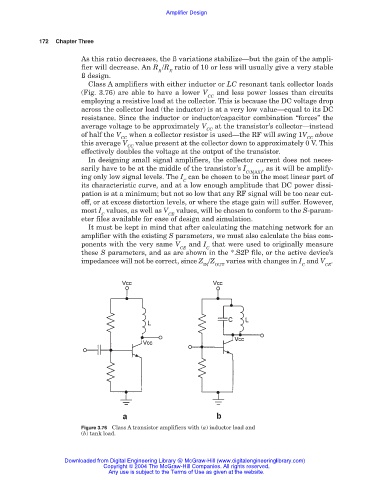
Class A amplifiers with either inductor or LC resonant tank collector loads
(Fig. 3.76) are able to have a lower V and less power losses than circuits
CC
employing a resistive load at the collector. This is because the DC voltage drop
across the collector load (the inductor) is at a very low value—equal to its DC
resistance. Since the inductor or inductor/capacitor combination “forces” the
average voltage to be approximately V at the transistor’s collector—instead
CC
of half the V when a collector resistor is used—the RF will swing 1V above
CC CC
this average V value present at the collector down to approximately 0 V. This
CC
effectively doubles the voltage at the output of the transistor.
In designing small signal amplifiers, the collector current does not neces-
sarily have to be at the middle of the transistor’s I , as it will be amplify-
C(MAX)
ing only low signal levels. The I can be chosen to be in the most linear part of
C
its characteristic curve, and at a low enough amplitude that DC power dissi-
pation is at a minimum; but not so low that any RF signal will be too near cut-
off, or at excess distortion levels, or where the stage gain will suffer. However,
most I values, as well as V values, will be chosen to conform to the S-param-
C CE
eter files available for ease of design and simulation.
It must be kept in mind that after calculating the matching network for an
amplifier with the existing S parameters, we must also calculate the bias com-
ponents with the very same V and I that were used to originally measure
CE C
these S parameters, and as are shown in the *.S2P file, or the active device’s
impedances will not be correct, since Z /Z varies with changes in I and V .
IN OUT C CE
Figure 3.76 Class A transistor amplifiers with (a) inductor load and
(b) tank load.
Downloaded from Digital Engineering Library @ McGraw-Hill (www.digitalengineeringlibrary.com)
Copyright © 2004 The McGraw-Hill Companies. All rights reserved.
Any use is subject to the Terms of Use as given at the website.