
Page 175 - Complete Wireless Design
P. 175
Amplifier Design
174 Chapter Three
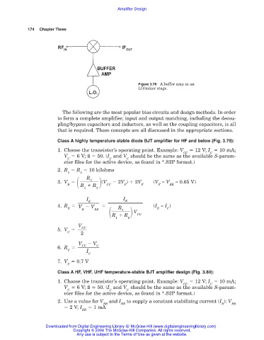
Figure 3.78 A buffer amp in an
LO/mixer stage.
The following are the most popular bias circuits and design methods. In order
to form a complete amplifier, input and output matching, including the decou-
pling/bypass capacitors and inductors, as well as the coupling capacitors, is all
that is required. These concepts are all discussed in the appropriate sections.
Class A highly temperature stable diode BJT amplifier for HF and below (Fig. 3.79):
1. Choose the transistor’s operating point. Example: V 12 V; I 10 mA;
CC C
V 6 V; ß 50. (I and V should be the same as the available S-param-
C C C
eter files for the active device, as found in *.S2P format.)
2. R R 10 kilohms
1 2
B R 2
3. V (V CC 2V ) 2V F (V ≈ V BE ≈ 0.65 V)
R R
F
F
1 2
I I E
E
4. R V V (I ≈ I )
V CC
E B BE R E C
2
R R
1 2
V
CC
5. V
C 2
V V
C
CC
6. R
C I
C
7. V 0.7 V
F
Class A HF, VHF, UHF temperature-stable BJT amplifier design (Fig. 3.80):
1. Choose the transistor’s operating point. Example: V 12 V; I 10 mA;
CC C
V 6 V; ß 50. (I and V should be the same as the available S-param-
C C C
eter files for the active device, as found in *.S2P format.)
2. Use a value for V and I to supply a constant stabilizing current (I ): V
BB BB B BB
2 V; I 1 mA
BB
Downloaded from Digital Engineering Library @ McGraw-Hill (www.digitalengineeringlibrary.com)
Copyright © 2004 The McGraw-Hill Companies. All rights reserved.
Any use is subject to the Terms of Use as given at the website.