
Page 180 - Complete Wireless Design
P. 180
Amplifier Design
Amplifier Design 179
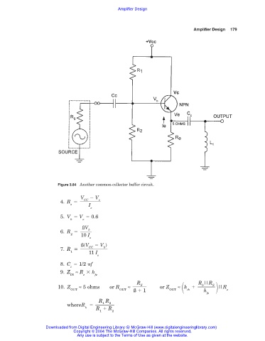
Figure 3.84 Another common-collector buffer circuit.
V V
CC
4. R e
e I
e
5. V V 0.6
b e
ßV
b
6. R
2 10 I
e
ß(V V )
b
CC
7. R
1 11 I
e
8. C 1/2 f
c
9. Z ≈ R h
IN e fe
R R ||R
S
10. Z ≈ 5 ohms or R ≈ or Z OUT b S ||R
≈ h
OUT OUT ß 1 ib h e
fe
R R
2
1
whereR
b R R
1 2
Downloaded from Digital Engineering Library @ McGraw-Hill (www.digitalengineeringlibrary.com)
Copyright © 2004 The McGraw-Hill Companies. All rights reserved.
Any use is subject to the Terms of Use as given at the website.