
Page 181 - Complete Wireless Design
P. 181
Amplifier Design
180 Chapter Three
h 0.025/I
ib e
R output impedance of the source
S
L , C match to 50 ohms
1 1
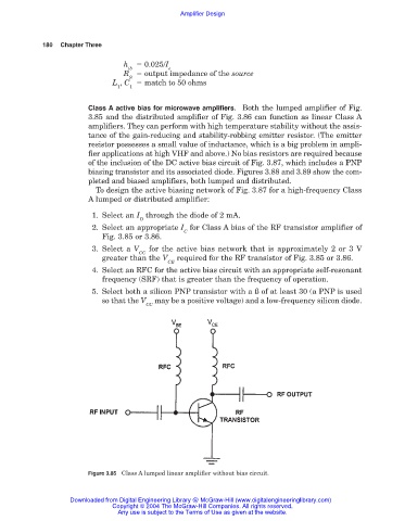
Class A active bias for microwave amplifiers. Both the lumped amplifier of Fig.
3.85 and the distributed amplifier of Fig. 3.86 can function as linear Class A
amplifiers. They can perform with high temperature stability without the assis-
tance of the gain-reducing and stability-robbing emitter resistor. (The emitter
resistor possesses a small value of inductance, which is a big problem in ampli-
fier applications at high VHF and above.) No bias resistors are required because
of the inclusion of the DC active bias circuit of Fig. 3.87, which includes a PNP
biasing transistor and its associated diode. Figures 3.88 and 3.89 show the com-
pleted and biased amplifiers, both lumped and distributed.
To design the active biasing network of Fig. 3.87 for a high-frequency Class
A lumped or distributed amplifier:
1. Select an I through the diode of 2 mA.
D
2. Select an appropriate I for Class A bias of the RF transistor amplifier of
C
Fig. 3.85 or 3.86.
3. Select a V for the active bias network that is approximately 2 or 3 V
CC
greater than the V required for the RF transistor of Fig. 3.85 or 3.86.
CE
4. Select an RFC for the active bias circuit with an appropriate self-resonant
frequency (SRF) that is greater than the frequency of operation.
5. Select both a silicon PNP transistor with a ß of at least 30 (a PNP is used
so that the V may be a positive voltage) and a low-frequency silicon diode.
CC
Figure 3.85 Class A lumped linear amplifier without bias circuit.
Downloaded from Digital Engineering Library @ McGraw-Hill (www.digitalengineeringlibrary.com)
Copyright © 2004 The McGraw-Hill Companies. All rights reserved.
Any use is subject to the Terms of Use as given at the website.