
Page 138 -
P. 138
APPENDIX 3A TIMING DIAGRAMS 109
Binary 1
Binary 0
Leading Trailing
edge edge Time gap Time
(a) Signal as a function of time
All lines Each line may All lines
at 0 be 0 or 1 at 0
(b) Groups of lines
Command
Response
(c) Cause-and-effect dependencies
(d) Clock signal
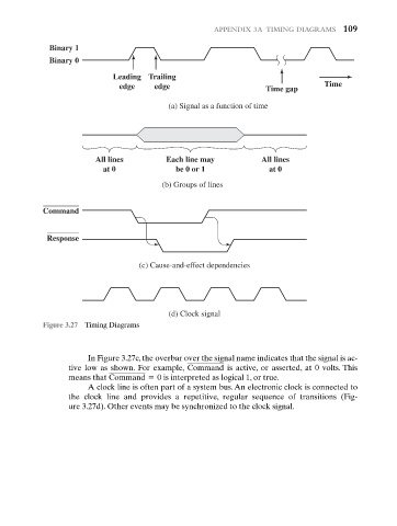
Figure 3.27 Timing Diagrams
In Figure 3.27c, the overbar over the signal name indicates that the signal is ac-
tive low as shown. For example, Command is active, or asserted, at 0 volts. This
means that Command = 0 is interpreted as logical 1, or true.
A clock line is often part of a system bus. An electronic clock is connected to
the clock line and provides a repetitive, regular sequence of transitions (Fig-
ure 3.27d). Other events may be synchronized to the clock signal.