
Page 174 -
P. 174
144 CHAPTER 4 / CACHE MEMORY
Table 4.6 ARM Cache Features
Cache Line Write
Cache Cache Size Size Buffer Size
Core Type (kB) (words) Associativity Location (words)
ARM720T Unified 8 4 4-way Logical 8
ARM920T Split 16/16 D/I 8 64-way Logical 16
ARM926EJ-S Split 4-128/4-128 D/I 8 4-way Logical 16
ARM1022E Split 16/16 D/I 8 64-way Logical 16
ARM1026EJ-S Split 4-128/4-128 D/I 8 4-way Logical 8
Intel
Split 16/16 D/I 4 32-way Logical 32
StrongARM
Intel Xscale Split 32/32 D/I 8 32-way Logical 32
ARM1136-JF-S Split 4-64/4-64 D/I 8 4-way Physical 32
Table 4.6 shows this evolution. The ARM7 models used a unified L1 cache,
while all subsequent models use a split instruction/data cache. All of the ARM de-
signs use a set-associative cache, with the degree of associativity and the line size
varying.ARM cached cores with an MMU use a logical cache for processor families
ARM7 through ARM10, including the Intel StongARM and Intel Xscale proces-
sors. The ARM11 family uses a physical cache. The distinction between logical and
physical cache is discussed earlier in this chapter (Figure 4.7).
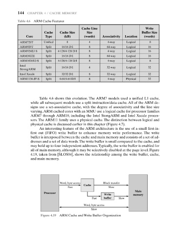
An interesting feature of the ARM architecture is the use of a small first-in-
first out (FIFO) write buffer to enhance memory write performance. The write
buffer is interposed between the cache and main memory and consists of a set of ad-
dresses and a set of data words.The write buffer is small compared to the cache, and
may hold up to four independent addresses.Typically, the write buffer is enabled for
all of main memory, although it may be selectively disabled at the page level. Figure
4.19, taken from [SLOS04], shows the relationship among the write buffer, cache,
and main memory.
Word, byte access Block transfer
Cache
Fast Slow
Main
Processor
Write memory
Fast buffer Slow
Word, byte access
Slow
Figure 4.19 ARM Cache and Write Buffer Organization