
Page 21 - DSP Integrated Circuits
P. 21
6 Chapter 1 DSP Integrated Circuits
cost of a slightly larger design effort. Large efforts are therefore being directed
toward automatic design of ASIC signal processors. Major drawbacks of this
approach are the inefficiency in terms of chip area and power consumption for
applications with small computational workloads, and its inability to meet the
throughput requirements in applications with high work loads.
1.4.2 Direct Mapping Techniques
Characteristic for direct mapping techniques is
that the DSP algorithm is mapped directly onto a
hardware structure without any intermediate rep-
resentation. The direct mapping approach is par-
ticularly suitable for implementing systems with a
fixed function, for example, digital filters. This
approach allows a perfect match between the DSP
algorithm, circuit architecture, and the system
requirements. However, algorithms with many
data-dependent branching operations may be
unsuited to this method. Such algorithms are more
easily implemented using the two approaches just
discussed. Fortunately, such branching operations
are rarely used in DSP algorithms.
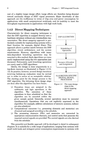
Ideally, the design is done sequentially in a
top-down manner, as illustrated in Figure 1.3 [5,
12]. In practice, however, several design iterations
involving bottom-up evaluation must be carried
out in order to arrive at an acceptable solution.
The starting point for the design process is the
DSP algorithm. The following three design steps
are done after the algorithm has been frozen. Figure 1.3 The major design
steps in the
Q Execution times are assigned to the
direct mapping
arithmetic and logic operations in the approach
algorithm. The execution of these
operations is then scheduled so that the
algorithm can be executed within the
given sample penod. Generally, several operations must be executed
simultaneously. Operations that are not explicitly expressed in the
algorithm (for example, address calculations of memory accesses, indices)
are also scheduled.
Q Computational resources (i.e., processing elements and memories) are
allocated and assigned according to the schedule.
Q The processing elements (PEs) and memories are connected by
appropriate communication channels, and control units that generate the
required control signals are provided. The control signals are also derived
from the schedule.
This powerful and flexible approach will be developed in detail in subsequent
chapters. It is suitable for a wide range of applications, ranging from systems with
small work loads and stringent power consumption requirements to systems with