
Page 547 - DSP Integrated Circuits
P. 547
532 Chapter 12 Integrated Circuit Design
is an important first step in the layout of an integrated circuit. It is the process of
determining the shapes and relative positions of the modules so that the chip size
becomes small and a desired aspect ratio of the chip is obtained. I/O pin locations,
timing constraints, power dissipation, temperature gradients, and wire density
estimates are other factors guiding the relative placement.
Most of the early systems developed for layout
focused on minimizing the chip area. However, perfor-
mance issues—in particular, speed and power con-
sumption have recently become a major concern.
Notice that a smaller chip represents a smaller capac-
itive load and may therefore be potentially faster and
consume less power than a larger chip. Floor planning
is used to verify the feasibility of a design without
performing the detailed layout and design of all the
blocks and functions.
The next step, referred to as placement, is deter-
mining the precise positions and orientations of the
modules. The goal is to complete the placement and
interconnections in the smallest possible area consis-
tent with a set of technological and performance con-
straints.
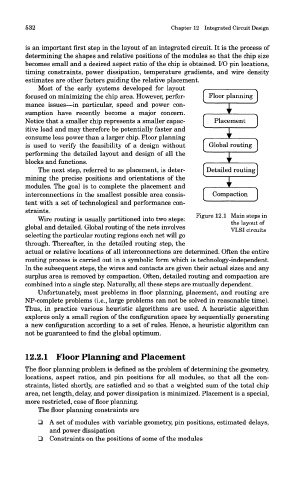
Figure 12.1 Main steps in
Wire routing is usually partitioned into two steps:
the layout of
global and detailed. Global routing of the nets involves
VLSI circuits
selecting the particular routing regions each net will go
through. Thereafter, in the detailed routing step, the
actual or relative locations of all interconnections are determined. Often the entire
routing process is carried out in a symbolic form which is technology-independent.
In the subsequent steps, the wires and contacts are given their actual sizes and any
surplus area is removed by compaction. Often, detailed routing and compaction are
combined into a single step. Naturally, all these steps are mutually dependent.
Unfortunately, most problems in floor planning, placement, and routing are
NP-complete problems (i.e., large problems can not be solved in reasonable time).
Thus, in practice various heuristic algorithms are used. A heuristic algorithm
explores only a small region of the configuration space by sequentially generating
a new configuration according to a set of rules. Hence, a heuristic algorithm can
not be guaranteed to find the global optimum.
12.2.1 Floor Planning and Placement
The floor planning problem is defined as the problem of determining the geometry,
locations, aspect ratios, and pin positions for all modules, so that all the con-
straints, listed shortly, are satisfied and so that a weighted sum of the total chip
area, net length, delay, and power dissipation is minimized. Placement is a special,
more restricted, case of floor planning.
The floor planning constraints are
Q A set of modules with variable geometry, pin positions, estimated delays,
and power dissipation
Q Constraints on the positions of some of the modules