
Page 180 - Electrical Properties of Materials
P. 180
162 Principles of semiconductor devices
(a)
p n
(b) Conduction band
donor levels
Fermi level
Fermi level
Acceptor Valence band
levels
(c)
(d)
N
h
N
e
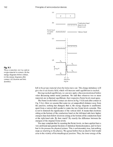
Fig. 9.1
Log N
The p–n junction. (a) A p- and an N h
n-type material in contact, (b) the
N
energy diagrams before contact, e
(c) the energy diagrams after
contact, (d) electron and hole Junction
densities. region
left in the p-type material when the holes move out. This charge imbalance will
give rise to an electric field, which will increase until equilibrium is reached.
Having reached equilibrium, we can now apply a theorem mentioned before
when discussing metal–metal junctions. We said that whenever two or more
materials are in thermal equilibrium, their respective Fermi levels must agree.
The Fermi levels before contact are shown in Fig. 9.1(b) and after contact in
Fig. 9.1(c). Here we assume that some (as yet unspecified) distance away from
the junction, nothing has changed; that is, the energy diagram is unaffected,
apart from a vertical shift needed to make the two Fermi levels coincide. This
is not to diminish the significance of the vertical shift. It means that electrons
sitting at the bottom of the conduction band on the left-hand side have higher
energies than their fellow electrons sitting at the bottom of the conduction band
at the right-hand side. By how much? By exactly the difference between the
energies of the original Fermi levels.
You may complain that by equating the Fermi levels, we have applied here a
very profound and general theorem of statistical thermodynamics, and we have
lost in the process the physical picture. This is unfortunately true, but nothing
stops us returning to the physics. We agreed before that an electric field would
arise in the vicinity of the metallurgical junction. Thus, the lower energy of the