
Page 182 - Electrical Properties of Materials
P. 182
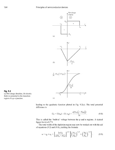
164                           Principles of semiconductor devices

                                                                 Net charge
                                                                 density
                                                          p       n
                                                             N
                                                              D
                                                         –x          +          x
                                                          p
                                                                           x
                                                                           n
                                                            –
                                                                –N A
                                                  (a)


                                                         –x p              x n   x


                                                                  eN x
                                                  (b)               D n
                                                                    ε


                                                                 U
                                                   e  (N x + N x )
                                                             2
                                                        2
                                                  2ε  A p  D n


                                                                 eN x 2
                                                                   A p
                                                                  2ε
     Fig. 9.2
     (a) Net charge densities, (b) electric             –x                 x   x
                                                         p                  n
     field, (c) potential in the transition
     region of a p–n junction.                    (c)

                                   leading to the quadratic function plotted in Fig. 9.2(c). The total potential
                                   difference is
                                                                          2
                                                                                2
                                                                     e(N A x + N D x )
                                                                                n
                                                                          p
                                                 U 0 = U(x n )– U(–x p )=         .          (9.8)
                                                                          2
                                   This is called the ‘built-in’ voltage between the p and n regions. A typical
                                   figure for it is 0.7 V.
                                     The total width of the depletion region may now be worked out with the aid
                                   of equations (9.2) and (9.8), yielding the formula


 1/2       1/2       1/2
                                                       2 U 0         N A       N D
                                        w = x p + x n =                     +          .     (9.9)
                                                     e(N A + N D )   N D       N A