
Page 183 - Electrical Properties of Materials
P. 183
The p–n junction in equilibrium 165
If, say, N A N D , eqn (9.9) reduces to
1/2
2 U 0
w = , (9.10)
eN D
which shows clearly that if the p-region is more highly doped, practically
all of the potential drop is in the n-region. Taking for the donor density
21
N D =10 m –3 and the typical figure of 0.7 V for the built-in voltage, the
width of the transition region in silicon (ε r = 11.9) comes to about 1 μm. Re-
member this is the value for an abrupt junction. In practice, the change from
acceptor impurities to donor impurities is gradual, and the transition region is
therefore much wider. Thus in a practical case we cannot very much rely on
the formulae derived above, but if we have an idea how the acceptor and donor
concentrations vary, similar equations can be derived.
From our simple model (assuming a depletion region) we obtained a
quadratic dependence of the potential energy in the transition region. More
complicated models give somewhat different dependence, but they all agree
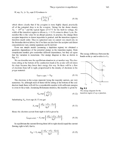
The energy difference between the
that the variation is monotonic. Our energy diagram is thus as shown in
Fig. 9.3. bands on the p- and n-sides is eU 0 .
We can describe now the equilibrium situation in yet another way. The elec-
trons sitting at the bottom of the conduction band at the p-side will roll down
the slope because they lower their energy this way. So there will be a flow eU
0
of electrons from left to right, proportional to the density of electrons in the
p-type material:
I e(left to right) ∼ N ep . (9.11) E g
The electrons in the n-type material, being the majority carriers, are very
numerous. So, although most of them will be sitting at the bottom of the con- 0
–x x
duction band, there will still be a considerable number with sufficient energies p n
to cross to the p-side. Assuming Boltzmann statistics, this number is given by Fig. 9.3
The energy diagram for the
–eU 0 transition region of a p–n junction.
N en exp . (9.12)
k B T
Substituting N en from eqn (8.17) we get
–(E g + eU 0 – E F )
N c exp . (9.13)
k B T
Hence the electron current from right to left is given by
–(E g + eU 0 – E F )
I e(right to left) ∼ N c exp . (9.14)
k B T
In equilibrium the current flowing from left to right should equal the current
flowing right to left; that is,
–(E g + eU 0 – E F )
N ep = N c exp . (9.15)
k B T