Page 184 - Electrical Properties of Materials
P. 184

166                           Principles of semiconductor devices

                                     Equation (9.15) gives nothing new. If we express the electron density in
                                   the p-type material with the aid of the Fermi level, then we could show from
                                   eqn (9.15) that eU 0 should be equal to the difference between the original
                                   Fermi levels, which we already knew. But although eqn (9.15) does not give any
                                   new information, we shall see in a moment that by describing the equilibrium
                                   in terms of currents flowing in opposite directions, the rectifying properties of
                                   the p–n junction can be easily understood.
                                     We could go through the same argument for holes without much difficulty,
                                   provided we can imagine particles rolling uphill, because for holes that is the
                                   way to lower their energy. The equations would look much the same, and I shall
                                   not bother to derive them.
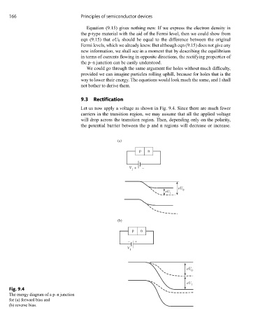
                                   9.3  Rectification

                                   Let us now apply a voltage as shown in Fig. 9.4. Since there are much fewer
                                   carriers in the transition region, we may assume that all the applied voltage
                                   will drop across the transition region. Then, depending only on the polarity,
                                   the potential barrier between the p and n regions will decrease or increase.


                                                  (a)

                                                           p  n


                                                       V +  –
                                                        1


                                                                           eU
                                                                      eU     0
                                                                        1


                                                  (b)
                                                        p  n

                                                      –  +
                                                      V
                                                       1


                                                                               eU
                                                                                0

                                                                               eU
                                                                                1
     Fig. 9.4
     The energy diagram of a p–n junction
     for (a) forward bias and
     (b) reverse bias.
   179   180   181   182   183   184   185   186   187   188   189