
Page 189 - Electrical Properties of Materials
P. 189
The transistor 171
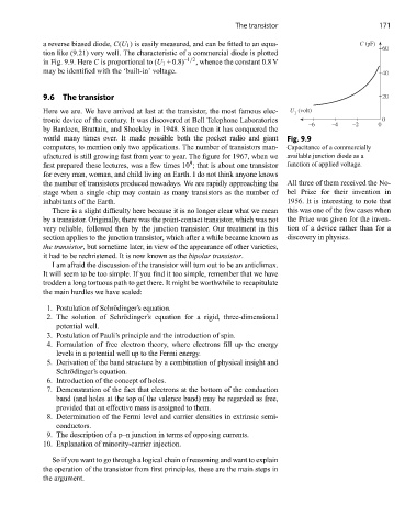
a reverse biased diode, C(U 1 ) is easily measured, and can be fitted to an equa- C (pF)
60
tion like (9.21) very well. The characteristic of a commercial diode is plotted
in Fig. 9.9. Here C is proportional to (U 1 +0.8) –1/2 , whence the constant 0.8 V
may be identified with the ‘built-in’ voltage. 40
9.6 The transistor 20
Here we are. We have arrived at last at the transistor, the most famous elec- U (volt)
1
tronic device of the century. It was discovered at Bell Telephone Laboratories 0
–6 –4 –2 0
by Bardeen, Brattain, and Shockley in 1948. Since then it has conquered the
world many times over. It made possible both the pocket radio and giant Fig. 9.9
computers, to mention only two applications. The number of transistors man- Capacitance of a commercially
ufactured is still growing fast from year to year. The figure for 1967, when we available junction diode as a
9
first prepared these lectures, was a few times 10 ; that is about one transistor function of applied voltage.
for every man, woman, and child living on Earth. I do not think anyone knows
the number of transistors produced nowadays. We are rapidly approaching the All three of them received the No-
stage when a single chip may contain as many transistors as the number of bel Prize for their invention in
inhabitants of the Earth. 1956. It is interesting to note that
There is a slight difficulty here because it is no longer clear what we mean this was one of the few cases when
by a transistor. Originally, there was the point-contact transistor, which was not the Prize was given for the inven-
very reliable, followed then by the junction transistor. Our treatment in this tion of a device rather than for a
section applies to the junction transistor, which after a while became known as discovery in physics.
the transistor, but sometime later, in view of the appearance of other varieties,
it had to be rechristened. It is now known as the bipolar transistor.
I am afraid the discussion of the transistor will turn out to be an anticlimax.
It will seem to be too simple. If you find it too simple, remember that we have
trodden a long tortuous path to get there. It might be worthwhile to recapitulate
the main hurdles we have scaled:
1. Postulation of Schrödinger’s equation.
2. The solution of Schrödinger’s equation for a rigid, three-dimensional
potential well.
3. Postulation of Pauli’s principle and the introduction of spin.
4. Formulation of free electron theory, where electrons fill up the energy
levels in a potential well up to the Fermi energy.
5. Derivation of the band structure by a combination of physical insight and
Schrödinger’s equation.
6. Introduction of the concept of holes.
7. Demonstration of the fact that electrons at the bottom of the conduction
band (and holes at the top of the valence band) may be regarded as free,
provided that an effective mass is assigned to them.
8. Determination of the Fermi level and carrier densities in extrinsic semi-
conductors.
9. The description of a p–n junction in terms of opposing currents.
10. Explanation of minority-carrier injection.
So if you want to go through a logical chain of reasoning and want to explain
the operation of the transistor from first principles, these are the main steps in
the argument.