
Page 191 - Electrical Properties of Materials
P. 191
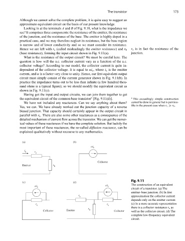
The transistor                        173

            Although we cannot solve the complete problem, it is quite easy to suggest an
            approximate equivalent circuit on the basis of our present knowledge.
               Looking in at the terminals A and B of Fig. 9.10, what is the impedance we
            see? It comprises three components: the resistance of the emitter, the resistance
            of the junction, and the resistance of the base. The emitter is highly doped in a
            practical case, and we may therefore neglect its resistance, but the base region
            is narrow and of lower conductivity and so we must consider its resistance.
                                                                             r e is in fact the resistance of the
            Hence we are left with r e (called misleadingly the emitter resistance) and r b
            (base resistance), forming the input circuit shown in Fig. 9.11(a).  junction.
               What is the resistance of the output circuit? We must be careful here. The
            question is how will the a.c. collector current vary as a function of the a.c.
            collector voltage? According to our model, the collector current is quite in-
            dependent of the collector voltage. It is equal to αi e , where i e is the emitter
            current, and α is a factor very close to unity. Hence, our first equivalent output
            circuit must simply consist of the current generator shown in Fig. 9.11(b). In
            practice the impedance turns out to be less than infinite (a few hundred thou-
            sand ohms is a typical figure); so we should modify the equivalent circuit as
            shown in Fig. 9.11(c).
               Having got the input and output circuits, we can join them together to get
                                                      ∗
            the equivalent circuit of the common base transistor [Fig. 9.11(d)].  ∗  This exceedingly simple construction
               We have not included any reactances. Can we say anything about them?  cannot be done in general but is permiss-
                                                                             ible in the present case when r c   r b .
            Yes, we can. We have already worked out the junction capacity of a reverse
            biased junction. That capacity should certainly appear in the output circuit in
            parallel with r c . There are also some other reactances as a consequence of the
            detailed mechanism of current flow across the transistor. We can get the numer-
            ical values of these reactances if we have the complete solution. But luckily the
            most important of these reactances, the so-called diffusion reactance, can be
            explained qualitatively without recourse to any mathematics.


              (a)                          (b)
                                                      αi e
               i
                e    r
                      e
                                                          Collector
              Emitter           r b


                                                                             Fig. 9.11
              (c)                          (d)
                     αi e                                     αi e           The construction of an equivalent
                                                                             circuit of a transistor. (a) The
                                                                             emitter–base junction. (b) In first
                                              r
                                               e                             approximation the collector current
                                                                             depends only on the emitter current.
                      r                                        r             (c) In a more accurate representation
                      c                                         c
                                                                             there is a collector resistance r c as
                                                    r
                          Collector     Emitter      b             Collector  well as the collector circuit. (d) The
                                                                             complete low-frequency equivalent
                                                                             circuit.