
Page 192 - Electrical Properties of Materials
P. 192
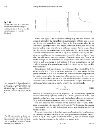
174                           Principles of semiconductor devices


     Fig. 9.12                                                        Emitter current
     The emitter current as a function of  Emitter voltage
     time when the emitter voltage is
     suddenly increased. It looks like the
     current response of a parallel
     RC circuit.                                              t                               t

                                     Let us look again at the p–n junction of the p–n–p transistor. When a step
                                   voltage is applied in the forward direction, the number of holes able to cross
                                   into the n-region suddenly increases. Thus, in the first moment, when the in-
                                   jected holes appear just inside the n-region, there is an infinite gradient of hole
                                   density, leading to an infinitely large diffusion current. As the holes diffuse
                                   into the n-region, the gradient decreases, and finally the current settles down
                                   to its new stationary value as shown in Fig. 9.12. But this is exactly the beha-
                                   viour one would expect from a capacitance in parallel with a resistance. Thus,
                                   when we wish to represent the variation of emitter current as a function of
                                   emitter voltage, we are entitled to put a capacitance there. This is not a real
                                   honest-to-god, capacitance; it just looks as if it were a capacitance, but that
                                   is all that matters. When drawing the equivalent circuit, we are interested in
                                   appearance only!
                                     Including now both capacitances, we get the equivalent circuit of Fig. 9.13.
                                   We are nearly there. There is one more important effect to consider: the fre-
                                   quency dependence of α. It is clear that the collector current is in phase with
                                   the emitter current when the transit time of the carriers across the base region
                                   is negligible, but α becomes complex (and its absolute value decreases) when
                                   this transit time is comparable with the period of the a.c. signal. We cannot go
     ∗  Not to depart from the usual notations,  into the derivation here, but α may be given by the simple formula ∗
     we are using j here as honest engineers
     do, but had we done the analysis with                        α 0
     our chosen exp(–iωt) time dependence,                 α =  1+j(ω/ω α ) ,               (9.22)
     we would have come up with –i instead
     of j.
                                   where ω α is called the alpha cut-off frequency. The corresponding equivalent
                                   circuit is obtained by replacing α in Fig. 9.13 by that given in eqn (9.22). And
                                   that is the end as far as we are concerned. Our final equivalent circuit represents
                                   fairly well the frequency dependence of a commercially available transistor.
                                     We have seen that the operation of the transistor can be easily under-
                                   stood by considering the current flow through it. The frequency dependence
                                   is more complicated, but still we have been able to point out how the various
                                   reactances arise.
                                     It has been convenient to describe the common base transistor configuration,
                                   but of course the most commonly used arrangement is the common emitter,
     †
      The full expression for i e should con-  shown in Fig. 9.14(a). Again, most of the current i e from the forward-biased
     tain a term dependent on the emitter-to-                                    †
     collector voltage. This is usually small.  emitter–base junction gets to the collector, so we can write
     Look it up in a circuitry book if you are
     interested in the finer details.                          i c = αi e ,                  (9.23)