
Page 196 - Electrical Properties of Materials
P. 196
178 Principles of semiconductor devices
φ - φ - eU
φ M M S 1
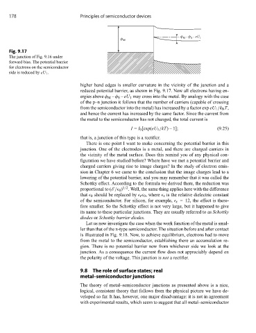
Fig. 9.17
The junction of Fig. 9.16 under
forward bias. The potential barrier
for electrons on the semiconductor
side is reduced by eU 1 .
higher band edges is smaller curvature in the vicinity of the junction and a
reduced potential barrier, as shown in Fig. 9.17. Now all electrons having en-
ergies above φ M – φ S – eU 1 may cross into the metal. By analogy with the case
of the p–n junction it follows that the number of carriers (capable of crossing
from the semiconductor into the metal) has increased by a factor exp eU 1 /k B T,
and hence the current has increased by the same factor. Since the current from
the metal to the semiconductor has not changed, the total current is
I = I 0 [exp(eU 1 /kT) – 1]; (9.25)
that is, a junction of this type is a rectifier.
There is one point I want to make concerning the potential barrier in this
junction. One of the electrodes is a metal, and there are charged carriers in
the vicinity of the metal surface. Does this remind you of any physical con-
figuration we have studied before? Where have we met a potential barrier and
charged carriers giving rise to image charges? In the study of electron emis-
sion in Chapter 6 we came to the conclusion that the image charges lead to a
lowering of the potential barrier, and you may remember that it was called the
Schottky effect. According to the formula we derived there, the reduction was
proportional to (E / 0 ) 1/2 . Well, the same thing applies here with the difference
that 0 should be replaced by r 0 , where r is the relative dielectric constant
of the semiconductor. For silicon, for example, r = 12, the effect is there-
fore smaller. So the Schottky effect is not very large, but it happened to give
its name to these particular junctions. They are usually referred to as Schottky
diodes or Schottky barrier diodes.
Let us now investigate the case when the work function of the metal is smal-
ler than that of the n-type semiconductor. The situation before and after contact
is illustrated in Fig. 9.18. Now, to achieve equilibrium, electrons had to move
from the metal to the semiconductor, establishing there an accumulation re-
gion. There is no potential barrier now from whichever side we look at the
junction. As a consequence the current flow does not appreciably depend on
the polarity of the voltage. This junction is not a rectifier.
9.8 The role of surface states; real
metal–semiconductor junctions
The theory of metal–semiconductor junctions as presented above is a nice,
logical, consistent theory that follows from the physical picture we have de-
veloped so far. It has, however, one major disadvantage: it is not in agreement
with experimental results, which seem to suggest that all metal–semiconductor