
Page 197 - Electrical Properties of Materials
P. 197
The role of surface states; real metal–semiconductor junctions 179
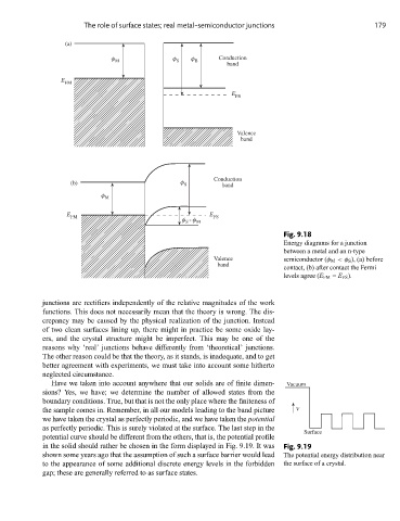
(a)
φ M φ S φ B Conduction
band
E
FM
E FS
Valence
band
Conduction
(b) φ S band
φ M
E E
FM FS
φ - φ M
S
Fig. 9.18
Energy diagrams for a junction
between a metal and an n-type
Valence semiconductor (φ M <φ S ), (a) before
band
contact, (b) after contact the Fermi
levels agree (E FM = E FS ).
junctions are rectifiers independently of the relative magnitudes of the work
functions. This does not necessarily mean that the theory is wrong. The dis-
crepancy may be caused by the physical realization of the junction. Instead
of two clean surfaces lining up, there might in practice be some oxide lay-
ers, and the crystal structure might be imperfect. This may be one of the
reasons why ‘real’ junctions behave differently from ‘theoretical’ junctions.
The other reason could be that the theory, as it stands, is inadequate, and to get
better agreement with experiments, we must take into account some hitherto
neglected circumstance.
Have we taken into account anywhere that our solids are of finite dimen- Vacuum
sions? Yes, we have; we determine the number of allowed states from the
boundary conditions. True, but that is not the only place where the finiteness of
the sample comes in. Remember, in all our models leading to the band picture V
we have taken the crystal as perfectly periodic, and we have taken the potential
as perfectly periodic. This is surely violated at the surface. The last step in the
Surface
potential curve should be different from the others, that is, the potential profile
in the solid should rather be chosen in the form displayed in Fig. 9.19. It was Fig. 9.19
shown some years ago that the assumption of such a surface barrier would lead The potential energy distribution near
to the appearance of some additional discrete energy levels in the forbidden the surface of a crystal.
gap; these are generally referred to as surface states.